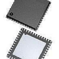
ASD5010L500INT Arctic Silicon Devices, ASD5010L500INT Datasheet - Page 32

ASD5010L500INT
Manufacturer Part Number
ASD5010L500INT
Description
ADC (A/D Converters) A-D Conv, Dig Gain Dual 8 bit 500MSPS
Manufacturer
Arctic Silicon Devices
Datasheet
1.ASD5010L500INT.pdf
(35 pages)
Specifications of ASD5010L500INT
Number Of Converters
2
Number Of Adc Inputs
4
Conversion Rate
500 MSPs
Resolution
8 bit
Snr
49.5 dB
Voltage Reference
1 V
Supply Voltage (max)
2 V
Supply Voltage (min)
1.7 V
Maximum Power Dissipation
295 mW
Maximum Operating Temperature
+ 85 C
Mounting Style
SMD/SMT
Package / Case
QFN-48
Input Voltage
1.8 V
Minimum Operating Temperature
- 40 C
Lead Free Status / RoHS Status
Lead free / RoHS Compliant
Preliminary Product Specification
side of the resistors may be used to provide dynamic
charging currents and may improve performance. The
resistors form a low pass filter with the capacitor, and
values must therefore be determined by requirements for
the application.
DC-Coupling
Figure 13 shows a recommended configuration for DC-
coupling. Note that the common mode input voltage must
be controlled according to specified values. Preferably,
the CM_EXT output should be used as reference to set
the common mode voltage.
The input amplifier could be inside a companion chip or it
could be a dedicated amplifier. Several suitable single
ended to differential driver amplifiers exist in the market.
The system designer should make sure the specifications
of the selected amplifier is adequate for the total system,
and that driving capabilities comply with ASD5010 input
specifications.
Detailed configuration and usage instructions must be
found in the documentation of the selected driver, and the
values given in figure 13 must be adjusted according to
the recommendations for the driver.
AC-Coupling
A signal transformer or series capacitors can be used to
make an AC-coupled input network. Figure 14 shows a
recommended configuration using a transformer. Make
sure that a transformer with sufficient linearity is selected,
and that the bandwidth of the transformer is appropriate.
The bandwidth should preferably exceed the sampling
rate of the ADC several times. It is also important to
minimize phase mismatch between the differential ADC
inputs for good HD2 performance. This type of
transformer coupled input is the preferred configuration
for high frequency signals as most differential amplifiers
do not have adequate performance at high frequencies.
Magnetic coupling between the transformers and PCB
traces may impact channel crosstalk, and must hence be
taken into account during PCB layout.
ASD5010
Input
Input
Figure 14: Transformer coupled input
Figure 13: DC coupled input
Input
Amplifier
R
47Ω
T
33 Ω
33 Ω
43 Ω
33 pF
43 Ω
CM_EXT
IPx
INx
CM_EXT
IPx
INx
rev 2.0, 2010.11.08
Page 32 of 35
If the input signal is traveling a long physical distance
from the signal source to the transformer (for example a
long cable), kick-backs from the ADC will also travel along
this distance. If these kick-backs are not terminated
properly at the source side, they are reflected and will add
to the input signal at the ADC input. This could reduce the
ADC performance. To avoid this effect, the source must
effectively terminate the ADC kick-backs, or the traveling
distance should be very short.
Figure 15 shows AC-coupling using capacitors. Resistors
from the CM_EXT output, R
differential input signals to the correct voltage. The series
capacitor, C
and the values must therefore be determined based on
the requirement to the high-pass cut-off frequency.
Note that Start Up Time from Sleep Mode and Power
Down Mode will be affected by this filter as the time
required to charge the series capacitors is dependent on
the filter cut-off frequency.
Clock Input and Jitter Considerations
Typically high-speed ADCs use both clock edges to
generate internal timing signals. In ASD5010 only the
rising edge of the clock is used.
The input clock can be supplied in a variety of formats.
The clock pins are AC-coupled internally, hence a wide
common mode voltage range is accepted. Differential
clock sources such as LVDS, LVPECL or differential sine
wave can be connected directly to the input pins. For
CMOS inputs, the CLKN pin should be connected to
ground, and the CMOS clock signal should be connected
to CLKP. For differential sine wave clock input the
amplitude must be at least +/- 0.8 Vpp. No additional
configuration is needed to set up the clock source format.
The quality of the input clock is extremely important for
high-speed, high-resolution ADCs. The contribution to
SNR from clock jitter with a full scale signal at a given
frequency is shown in equation 1.
where f
jitter measured in seconds. The rms jitter is the total of all
jitter sources including the clock generation circuitry, clock
distribution and internal ADC circuitry.
For applications where jitter may limit the obtainable
performance, it is of utmost importance to limit the clock
jitter. This can be obtained by using precise and stable
clock references (e.g. crystal oscillators with good jitter
specifications) and make sure the clock distribution is well
controlled. It might be advantageous to use analog power
and ground planes to ensure low noise on the supplies to
IN
is the signal frequency, and ε
INPx
INNx
SNR
I
, form the high-pass pole with these resistors,
Figure 15: AC coupled input
C
C
jitter
I
I
=20⋅log
22 Ω
22 Ω
R
R
CM
CM
CM
, should be used to bias the
2⋅⋅ f
22 pF
CM_EXT
IPx
INx
IN
t
is the total rms
⋅
t
Confidential
(1)


