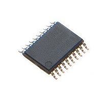
MAX1441GUP/V+ Maxim Integrated Products, MAX1441GUP/V+ Datasheet - Page 2

MAX1441GUP/V+
Manufacturer Part Number
MAX1441GUP/V+
Description
Touch Screen Converters & Controllers PROXIMITY SENSR el Proximity and Tou
Manufacturer
Maxim Integrated Products
Datasheet
1.MAX1441GUPV.pdf
(41 pages)
Specifications of MAX1441GUP/V+
Lead Free Status / RoHS Status
Lead free / RoHS Compliant
Automotive, Two-Channel Proximity and
Touch Sensor
ABSOLUTE MAXIMUM RATINGS
(V
V
V
SINPUT1, SINPUT2, AGUD1,
RESET, P0._, I.C. to DGND ...................... -0.3V to (V
AGND to DGND ...................................................-0.3V to +0.3V
OUT1, OUT2 to AGND ..........................................-0.3V to +28V
OUT_, P0._ Continuous Output Current .........................P 20mA
Continuous Power Dissipation (T
Note 1: Package thermal resistances were obtained using the method described in JEDEC specification JESD51-7, using a four-
Stresses beyond those listed under “Absolute Maximum Ratings” may cause permanent damage to the device. These are stress ratings only, and functional
operation of the device at these or any other conditions beyond those indicated in the operational sections of the specifications is not implied. Exposure to absolute
maximum rating conditions for extended periods may affect device reliability.
ELECTRICAL CHARACTERISTICS
(V
erwise noted.) (Note 2)
2
Average Power-Supply Current
CAPACITANCE-TO-DIGITAL CONVERTER
Bit Resolution
Input Capacitance Range
Input Capacitance LSB
Resolution
Integral Nonlinearity
Differential Nonlinearity
Sampling Time
Number of Effective Bits
DC Input Current of SINPUT1,
SINPUT2
INPUT CAPACITANCE EXCITATION SOURCE
Source Peak-to-Peak Voltage
Minimum Excitation Frequency
BATT
AA
DD
AGUD2 to AGND ...................................-0.3V to (V
Single-Layer PCB
20-Lead TSSOP (derate 11mW/NC above +70NC).......879mW
Multilayer PCB
20-Lead TSSOP (derate 13.6mW/NC above +70NC)..1084mW
BATT
, V
= V
DD
to AGND .....................................................-0.3V to +45V
= 5V to 28V, V
layer board. For detailed information on package thermal considerations, refer to
AA
to AGND ..................................................-0.3V to +4V
PARAMETER
, AGND = DGND, unless otherwise noted.)
AA
= V
DD
, T
A
= +70NC)
A
= -40NC to +105NC. Typical values are at V
SYMBOL
f
EXMIN
DNL
INL
16ms capacitance-to-digital (C2D) con-
version time, two active channels; CPU in
sleep mode
CRNG_[1:0] = 10
CRNG_[1:0] = 01
CRNG_[1:0] = 00
20pF capacitance range
10pF capacitance range
5pF capacitance range
f
300kHz excitation frequency
Frequency Control register = 0x0A (Note 3)
EX
DD
AA
= 300kHz (Note 3)
+ 0.3V)
+ 0.3V)
CONDITIONS
Junction-to-Case Thermal Resistance (B
Junction-to-Ambient Thermal Resistance (B
Operating Temperature Range ........................ -40NC to +105NC
Junction Temperature .....................................................+150NC
Storage Temperature Range ............................ -65NC to +150NC
Lead Temperature (soldering, 10s) ................................+300NC
Soldering Temperature (reflow) ......................................+260NC
20-Lead TSSOP ........................................................ +20NC/W
Single-Layer PCB
20-Lead TSSOP ........................................................ +91NC/W
Multilayer PCB
20-Lead TSSOP ..................................................... +73.8NC/W
BATT
= 14V, f
www.maxim-ic.com/thermal-tutorial
EX
0.96
MIN
= 300kHz, T
584
TYP
100
600
300
100
4.8
2.4
1.2
0.5
1.0
12
20
10
11
5
1
JC
A
= +25NC, unless oth-
) (Note 1)
JA
) (Note 1)
MAX
1.21
120
624
UNITS
%FS
V
LSB
Bits
Bits
kHz
FA
nA
pF
Fs
fF
P-P
.


