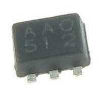
BD2270HFV-TR Rohm Semiconductor, BD2270HFV-TR Datasheet - Page 7

BD2270HFV-TR
Manufacturer Part Number
BD2270HFV-TR
Description
MOSFET & Power Driver ICs MOSFET Controller IC For Load Switching
Manufacturer
Rohm Semiconductor
Type
MOSFET Controller ICr
Specifications of BD2270HFV-TR
Package / Case
HVSOF-5
Product
MOSFET Gate Drivers
Rise Time
130 us
Fall Time
18 us
Supply Voltage (max)
5.5 V
Supply Voltage (min)
2.7 V
Supply Current
50 uA
Maximum Operating Temperature
+ 85 C
Mounting Style
SMD/SMT
Minimum Operating Temperature
- 25 C
Output Voltage
9.5 V
Primary Input Voltage
5.5V
No. Of Outputs
1
Voltage Regulator Case Style
HVSOF
No. Of Pins
5
Operating Temperature Range
-25°C To +85°C
Svhc
No SVHC (18-Jun-2010)
Base
RoHS Compliant
Lead Free Status / RoHS Status
Lead free / RoHS Compliant
Lead Free Status / RoHS Status
Lead free / RoHS Compliant
Available stocks
Company
Part Number
Manufacturer
Quantity
Price
●Functional Description
© 2009 ROHM Co., Ltd. All rights reserved.
BD2270HFV
www.rohm.com
2.
3.
The BD2270HVF is a driver IC to use an N-channel MOSFET as a high side load switch. This IC incorporates the following
functions.
1. GATE drive
4. Analog control input terminal
A voltage to drive the gate of N-channel MOSFET is generated by a built-in charge pump in the BD2270HFV. The built-in
charge pump in the BD2270HFV generates a voltage three times as high as the power supply voltage at the GATE
terminal. In addition, since this IC has a built-in capacitor for the charge pump, it needs no external parts.
The charge pump operates when the AEN is set to High. When the AEN is set to Low, the GATE terminal voltage is fixed
to the GND level.
The output discharge circuit is enabled when the AEN is set to Low. When the discharge circuit is activated, the
200Ω(Typ.) MOSFET switch located between the DISC terminal and the GND terminal turns ON. Connecting between the
DISC terminal and the source side (load side) of the N-channel MOSFET makes it possible to immediately discharge
capacitive load.
When the AEN terminal input voltage reaches the High level, the built-in charge pump in the BD2270HFV charges the
gate of the N-channel MOSFET. The turn-on time of the N-channel MOSFET is determined by the GATE capacity. In
addition, connecting a capacitor to the GATE terminal makes it possible to slow the rise of turn-on time of the N-channel
MOSFET, thus achieving reduction of the inrush current to a large capacitive load.
The AEN input of the BD2270HFV is connected to the built-in hysteresis comparator. Consequently, even analog signals
can control the BD2270HFV, thus facilitating the control of the switch ON-OFF sequence.
Output discharge circuit
Soft start function
* To turn ON the power supply (V
Discharge circuit
V
OUT_SWITCH
V
放電回路
IN_SWITCH
V
V
GATE
V
AEN
CC
CC
, VIN
ON
_SWITCH
), set the AEN to Low.
Fig. 34 Operation Timing
7/12
OFF
ON
Technical Note
2009.04 - Rev.A


