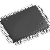
LFEC3E-3QN208C Lattice, LFEC3E-3QN208C Datasheet - Page 14

LFEC3E-3QN208C
Manufacturer Part Number
LFEC3E-3QN208C
Description
FPGA - Field Programmable Gate Array 3.1K LUTs
Manufacturer
Lattice
Datasheet
1.LFEC3E-5TN144C.pdf
(163 pages)
Specifications of LFEC3E-3QN208C
Number Of Macrocells
3100
Number Of Programmable I/os
145
Data Ram Size
56320
Supply Voltage (max)
1.26 V
Maximum Operating Temperature
+ 100 C
Minimum Operating Temperature
- 40 C
Mounting Style
SMD/SMT
Supply Voltage (min)
1.14 V
Package / Case
PQFP-208
Lead Free Status / RoHS Status
Lead free / RoHS Compliant
Available stocks
Company
Part Number
Manufacturer
Quantity
Price
Company:
Part Number:
LFEC3E-3QN208C
Manufacturer:
Lattice
Quantity:
135
Company:
Part Number:
LFEC3E-3QN208C
Manufacturer:
Lattice Semiconductor Corporation
Quantity:
10 000
Part Number:
LFEC3E-3QN208C
Manufacturer:
LATTICE
Quantity:
20 000
- Current page: 14 of 163
- Download datasheet (962Kb)
Lattice Semiconductor
Table 2-5. PLL Signal Descriptions
For more information about the PLL, please see the list of technical documentation at the end of this data sheet.
Dynamic Clock Select (DCS)
The DCS is a global clock buffer with smart multiplexer functions. It takes two independent input clock sources and
outputs a clock signal without any glitches or runt pulses. This is achieved regardless of where the select signal is
toggled. There are eight DCS blocks per device, located in pairs at the center of each side. Figure 2-13 illustrates
the DCS Block Macro.
Figure 2-13. DCS Block Primitive
Figure 2-14 shows timing waveforms of the default DCS operating mode. The DCS block can be programmed to
other modes. For more information about the DCS, please see the list of technical documentation at the end of this
data sheet.
CLKI
CLKFB
RST
CLKOS
CLKOP
CLKOK
LOCK
DDAMODE
DDAIZR
DDAILAG
DDAIDEL[2:0]
DDAOZR
DDAOLAG
DDAODEL[2:0]
Signal
I/O
O
O
O
O
O
O
O
I
I
I
I
I
I
I
Clock input from external pin or routing
PLL feedback input from CLKOP (PLL internal), from clock net (CLKOP) or from a user clock
(PIN or logic)
“1” to reset PLL
PLL output clock to clock tree (phase shifted/duty cycle changed)
PLL output clock to clock tree (No phase shift)
PLL output to clock tree through secondary clock divider
“1” indicates PLL LOCK to CLKI
Dynamic Delay Enable. “1”: Pin control (dynamic), “0”: Fuse Control (static)
Dynamic Delay Zero. “1”: delay = 0, “0”: delay = on
Dynamic Delay Lag/Lead. “1”: Lead, “0”: Lag
Dynamic Delay Input
Dynamic Delay Zero Output
Dynamic Delay Lag/Lead Output
Dynamic Delay Output
CLK0
CLK1
SEL
DCS
2-11
DCSOUT
Description
LatticeECP/EC Family Data Sheet
Architecture
Related parts for LFEC3E-3QN208C
Image
Part Number
Description
Manufacturer
Datasheet
Request
R

Part Number:
Description:
FPGA - Field Programmable Gate Array 3.1K LUTs 97 IO 1.2V -3 Spd I
Manufacturer:
Lattice

Part Number:
Description:
FPGA - Field Programmable Gate Array 3.1K LUTs 67 IO 1.2V -3 Spd I
Manufacturer:
Lattice

Part Number:
Description:
FPGA - Field Programmable Gate Array 3.1K LUTs 145 IO 1.2 V -3 Spd I
Manufacturer:
Lattice
Part Number:
Description:
FPGA LatticeEC Family 3100 Cells 340MHz 130nm (CMOS) Technology 1.2V 256-Pin FBGA
Manufacturer:
LATTICE SEMICONDUCTOR
Datasheet:

Part Number:
Description:
FPGA - Field Programmable Gate Array 3.1K LUTs Pb-Free
Manufacturer:
Lattice
Datasheet:

Part Number:
Description:
FPGA LatticeEC Family 3100 Cells 340MHz 130nm (CMOS) Technology 1.2V 256-Pin FBGA
Manufacturer:
Lattice
Datasheet:

Part Number:
Description:
IC FPGA 3.1KLUTS 67I/O 100-TQFP
Manufacturer:
Lattice
Datasheet:

Part Number:
Description:
IC FPGA 3.1KLUTS 97I/O 144-TQFP
Manufacturer:
Lattice
Datasheet:

Part Number:
Description:
IC FPGA 3.1KLUTS 97I/O 144-TQFP
Manufacturer:
Lattice
Datasheet:

Part Number:
Description:
IC FPGA 3.1KLUTS 160I/O 256-BGA
Manufacturer:
Lattice
Datasheet:

Part Number:
Description:
IC FPGA 3.1KLUTS 67I/O 100-TQFP
Manufacturer:
Lattice
Datasheet:

Part Number:
Description:
IC FPGA 3.1KLUTS 145I/O 208-PQFP
Manufacturer:
Lattice
Datasheet:

Part Number:
Description:
IC FPGA 3KLUTS 208PQFP
Manufacturer:
Lattice
Datasheet:

Part Number:
Description:
IC FPGA 3.1KLUTS 160I/O 256-BGA
Manufacturer:
Lattice
Datasheet:

Part Number:
Description:
IC FPGA 3.1KLUTS 160I/O 256-BGA
Manufacturer:
Lattice
Datasheet:


