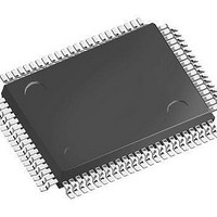
LFEC3E-3QN208C Lattice, LFEC3E-3QN208C Datasheet - Page 44

LFEC3E-3QN208C
Manufacturer Part Number
LFEC3E-3QN208C
Description
FPGA - Field Programmable Gate Array 3.1K LUTs
Manufacturer
Lattice
Datasheet
1.LFEC3E-5TN144C.pdf
(163 pages)
Specifications of LFEC3E-3QN208C
Number Of Macrocells
3100
Number Of Programmable I/os
145
Data Ram Size
56320
Supply Voltage (max)
1.26 V
Maximum Operating Temperature
+ 100 C
Minimum Operating Temperature
- 40 C
Mounting Style
SMD/SMT
Supply Voltage (min)
1.14 V
Package / Case
PQFP-208
Lead Free Status / RoHS Status
Lead free / RoHS Compliant
Available stocks
Company
Part Number
Manufacturer
Quantity
Price
Company:
Part Number:
LFEC3E-3QN208C
Manufacturer:
Lattice
Quantity:
135
Company:
Part Number:
LFEC3E-3QN208C
Manufacturer:
Lattice Semiconductor Corporation
Quantity:
10 000
Part Number:
LFEC3E-3QN208C
Manufacturer:
LATTICE
Quantity:
20 000
- Current page: 44 of 163
- Download datasheet (962Kb)
Lattice Semiconductor
Differential HSTL and SSTL
Differential HSTL and SSTL outputs are implemented as a pair of complementary single-ended outputs. All allow-
able single-ended output classes (class I and class II) are supported in this mode.
LVDS25E
The top and bottom side of LatticeECP/EC devices support LVDS outputs via emulated complementary LVCMOS
outputs in conjunction with a parallel resistor across the driver outputs. The scheme shown in
Figure 3-1 is one possible solution for point-to-point signals.
Figure 3-1. LVDS25E Output Termination Example
Table 3-1. LVDS25E DC Conditions
VCCIO = 2.5V (±5%)
VCCIO = 2.5V (±5%)
V
V
V
V
Z
OH
OL
OD
BACK
CM
Parameter
ON-chip
Output high voltage
Output low voltage
Output differential voltage
Output common mode voltage
Back impedance
OFF-chip
CAT16-LV4F12
RS=165 ohms
(±1%)
RS=165 ohms
(±1%)
Bourns
Transmission line, Zo = 100 ohm differential
Description
RD = 140 ohms
(±1%)
3-8
DC and Switching Characteristics
Typical
LatticeECP/EC Family Data Sheet
RD = 100 ohms
(±1%)
1.42
1.08
0.35
1.25
100
OFF-chip ON-chip
Units
V
V
V
V
Ω
+
-
Related parts for LFEC3E-3QN208C
Image
Part Number
Description
Manufacturer
Datasheet
Request
R

Part Number:
Description:
FPGA - Field Programmable Gate Array 3.1K LUTs 97 IO 1.2V -3 Spd I
Manufacturer:
Lattice

Part Number:
Description:
FPGA - Field Programmable Gate Array 3.1K LUTs 67 IO 1.2V -3 Spd I
Manufacturer:
Lattice

Part Number:
Description:
FPGA - Field Programmable Gate Array 3.1K LUTs 145 IO 1.2 V -3 Spd I
Manufacturer:
Lattice
Part Number:
Description:
FPGA LatticeEC Family 3100 Cells 340MHz 130nm (CMOS) Technology 1.2V 256-Pin FBGA
Manufacturer:
LATTICE SEMICONDUCTOR
Datasheet:

Part Number:
Description:
FPGA - Field Programmable Gate Array 3.1K LUTs Pb-Free
Manufacturer:
Lattice
Datasheet:

Part Number:
Description:
FPGA LatticeEC Family 3100 Cells 340MHz 130nm (CMOS) Technology 1.2V 256-Pin FBGA
Manufacturer:
Lattice
Datasheet:

Part Number:
Description:
IC FPGA 3.1KLUTS 67I/O 100-TQFP
Manufacturer:
Lattice
Datasheet:

Part Number:
Description:
IC FPGA 3.1KLUTS 97I/O 144-TQFP
Manufacturer:
Lattice
Datasheet:

Part Number:
Description:
IC FPGA 3.1KLUTS 97I/O 144-TQFP
Manufacturer:
Lattice
Datasheet:

Part Number:
Description:
IC FPGA 3.1KLUTS 160I/O 256-BGA
Manufacturer:
Lattice
Datasheet:

Part Number:
Description:
IC FPGA 3.1KLUTS 67I/O 100-TQFP
Manufacturer:
Lattice
Datasheet:

Part Number:
Description:
IC FPGA 3.1KLUTS 145I/O 208-PQFP
Manufacturer:
Lattice
Datasheet:

Part Number:
Description:
IC FPGA 3KLUTS 208PQFP
Manufacturer:
Lattice
Datasheet:

Part Number:
Description:
IC FPGA 3.1KLUTS 160I/O 256-BGA
Manufacturer:
Lattice
Datasheet:

Part Number:
Description:
IC FPGA 3.1KLUTS 160I/O 256-BGA
Manufacturer:
Lattice
Datasheet:


