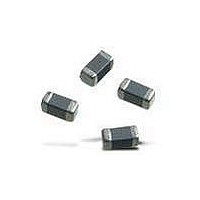
BLM21BD272SH1L Murata, BLM21BD272SH1L Datasheet - Page 70

BLM21BD272SH1L
Manufacturer Part Number
BLM21BD272SH1L
Description
EMI/RFI Suppressors & Ferrites 0805 2.7Kohms HiSpd Signal Line Tape
Manufacturer
Murata
Series
BLM Br
Datasheet
1.BLM18AG471SH1D.pdf
(93 pages)
Specifications of BLM21BD272SH1L
Shielding
Unshielded
Test Frequency
100 MHz
Product
Chip Ferrite Beads
Impedance
2.7 KOhms
Tolerance
25 %
Maximum Dc Current
200 mAmps
Maximum Dc Resistance
0.8 Ohms
Operating Temperature Range
- 55 C to + 125 C
Package / Case
0805 (2012 metric)
Termination Style
SMD/SMT
Dc Resistance Max
0.8ohm
Dc Current Rating
200mA
Ferrite Mounting
SMD
Ferrite Case Style
0805 / 2012
Operating Temperature Max
+125°C
Operating Temperature Min
-55°C
Rohs Compliant
Yes
Lead Free Status / RoHS Status
Lead free / RoHS Compliant
Available stocks
Company
Part Number
Manufacturer
Quantity
Price
Company:
Part Number:
BLM21BD272SH1L
Manufacturer:
MURATA
Quantity:
240 000
4
!Note
• This PDF catalog is downloaded from the website of Murata Manufacturing co., ltd. Therefore, it’s specifications are subject to change or our products in it may be discontinued without advance notice. Please check with our
• This PDF catalog has only typical specifications because there is no space for detailed specifications. Therefore, please approve our product specifications or transact the approval sheet for product specifications before ordering.
sales representatives or product engineers before ordering.
!Note
2. Solder Paste Printing and Adhesive Application
68
Chip EMIFILr (Soldering and Mounting)
DLW31S
DLW43S
BLM15
BLM18
BLM21
BLM31
BLM41
When reflow soldering the chip EMI suppression filter, the
printing must be conducted in accordance with the
following cream solder printing conditions.
If too much solder is applied, the chip will be prone to
damage by mechanical and thermal stress from the PCB
and may crack. In contrast, if too little solder is applied,
there is the potential that the termination strength will be
insufficient, creating the potential for detachment.
Standard land dimensions should be used for resist and
Continued from the preceding page.
• Please read rating and !CAUTION (for storage, operating, rating, soldering, mounting and handling) in this catalog to prevent smoking and/or burning, etc.
• This catalog has only typical specifications because there is no space for detailed specifications. Therefore, please approve our product specifications or transact the approval sheet for product specifications before ordering.
Series
oEnsure that solder is applied smoothly to a
oCoat the solder paste a thickness: 100-200 m
oReflow Soldering
oReflow Soldering
DLW31S
DLW43SH510XK2
DLW43SH101XK2
DLW43SH101XP2
minimum height of 0.2mm to 0.3mm at the end
surface of the part.
Series
Series
5.9
a
b
a
3
3
Solder Paste Printing
1.6
a
3.0
3.2
a
3.7
b
0.4
c
1.6
d
copper foil patterns.
When flow soldering the EMI suppression filter, apply the
adhesive in accordance with the following conditions.
If too much adhesive is applied, then it may overflow into
the land or termination areas and yield poor solderability.
In contrast, if insufficient adhesive is applied, or if the
adhesive is not sufficiently hardened, then the chip may
become detached during flow soldering process.
Do not use gilded pattern; excess soldering heat may dissolve
metal of a copper wire.
Do not use gilded pattern; excess soldering heat may dissolve
metal of a copper wire.
1 : If the pattern is made with wider than 1.6mm (DLW31S) it
2 : If the pattern is made with less than 0.4mm, in the worst
3 : If the pattern is made with wider than 1.6mm (DLW31S),
1 : If the pattern is made with wider than 3.4mm, it may result
2 : If the pattern is made with less than 1.6mm, in the worst
3 : If the pattern is made with wider, the strength of bending
may result in components turning around, because
melting speed is different. In the worst case, short circuit
between lines may occur.
case, short circuit between lines may occur due to spread
of soldering paste or mount placing accuracy.
the bending strength will be reduced.
in components turning around, because melting speed is
different. In the worst case, short circuit between lines
may be occur.
case, short circuit between lines may occur due to the
spread of soldering paste or mount placing accuracy.
will be reduced.
Coating amount is illustrated in the
following diagram.
PCB
Adhesive Application
Chip Solid Inductor
Land
Bonding agent
Continued on the following page.
Land Pattern
+ Solder Resist
Land Pattern
Solder Resist
a:20 70 m
b:30 35 m
c:50 105 m
a
b
(in mm)
(in mm)
c
C50E.pdf
08.8.28


