STL11N3LLH6 STMicroelectronics, STL11N3LLH6 Datasheet
STL11N3LLH6
Specifications of STL11N3LLH6
Available stocks


Related parts for STL11N3LLH6


STL11N3LLH6 Summary of contents
Page 1
... Order code STL11N3LLH6 September 2010 STripFET™ VI DeepGATE™ Power MOSFET R DS(on max. 0.0075 Ω ( DS(on) Figure 1. Marking 11N3L PowerFLAT™ (3.3 x 3.3) Doc ID 17755 Rev 1 STL11N3LLH6 PowerFLAT™ (3.3 x 3.3) Internal schematic diagram Package Packaging Tape and reel 1/10 www.st.com 10 ...
Page 2
... Contents Contents 1 Electrical ratings . . . . . . . . . . . . . . . . . . . . . . . . . . . . . . . . . . . . . . . . . . . . 3 2 Electrical characteristics . . . . . . . . . . . . . . . . . . . . . . . . . . . . . . . . . . . . . 4 3 Test circuits 4 Package mechanical data . . . . . . . . . . . . . . . . . . . . . . . . . . . . . . . . . . . . . 7 5 Revision history . . . . . . . . . . . . . . . . . . . . . . . . . . . . . . . . . . . . . . . . . . . . 9 2/ Doc ID 17755 Rev 1 STL11N3LLH6 ...
Page 3
... STL11N3LLH6 1 Electrical ratings Table 2. Absolute maximum ratings Symbol V Drain-source voltage ( Gate-source voltage GS (1) I Drain current (continuous (1) I Drain current (continuous (2) I Drain current (pulsed) DM (3) P Total dissipation at T TOT (1) P Total dissipation at T TOT Derating factor T Operating junction temperature J Storage temperature ...
Page 4
... 4 (see Figure 3) f=1 MHz Gate DC Bias = 0 Test signal level = 20 mV open drain Parameter Test conditions 4.7 Ω (see Figure 2) Doc ID 17755 Rev 1 STL11N3LLH6 Min. Typ. Max ± = 250 µ 5.5 A 0.006 0.0075 D = 5.5 A 0.0084 0.0095 D Min. Typ. Max. 1690 290 176 ...
Page 5
... STL11N3LLH6 Table 8. Source drain diode Symbol I Source-drain current SD (1) I Source-drain current (pulsed) SDM (2) V Forward on voltage SD t Reverse recovery time rr Q Reverse recovery charge rr I Reverse recovery current RRM 1. Pulse width limited by safe operating area 2. Pulsed: pulse duration=300µs, duty cycle 1.5% ...
Page 6
... Figure 5. 3.3 1000 µF µ AM01470v1 Figure 7. V (BR)DSS 10% 0 AM01472v1 Doc ID 17755 Rev 1 STL11N3LLH6 Gate charge test circuit 12V 47kΩ 100nF I =CONST G 100Ω GMAX 2200 µF 2.7kΩ 47kΩ 1kΩ Unclamped inductive load test circuit 2200 3.3 µ ...
Page 7
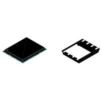
... STL11N3LLH6 4 Package mechanical data In order to meet environmental requirements, ST offers these devices in different grades of ® ECOPACK packages, depending on their level of environmental compliance. ECOPACK specifications, grade definitions and product status are available at: www.st.com. ECOPACK trademark. Doc ID 17755 Rev 1 Package mechanical data ® 7/10 ...
Page 8
... Doc ID 17755 Rev 1 STL11N3LLH6 inch MIN. TYP. MAX. 0.031 0.035 0.039 0.0007 0.0019 0.007 0.009 0.011 0.015 0.012 0.004 0.13 0.098 0.104 0.108 ...
Page 9
... STL11N3LLH6 5 Revision history Table 9. Document revision history Date 02-Sep-2010 Revision 1 First release Doc ID 17755 Rev 1 Revision history Changes 9/10 ...
Page 10
... Australia - Belgium - Brazil - Canada - China - Czech Republic - Finland - France - Germany - Hong Kong - India - Israel - Italy - Japan - Malaysia - Malta - Morocco - Philippines - Singapore - Spain - Sweden - Switzerland - United Kingdom - United States of America 10/10 Please Read Carefully: © 2010 STMicroelectronics - All rights reserved STMicroelectronics group of companies www.st.com Doc ID 17755 Rev 1 STL11N3LLH6 ...