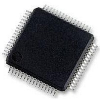
MC56F8257VLH Freescale Semiconductor, MC56F8257VLH Datasheet - Page 35

MC56F8257VLH
Manufacturer Part Number
MC56F8257VLH
Description
DSC 64K FLASH 60MHZ 64-LQFP
Manufacturer
Freescale Semiconductor
Series
56F8xxxr
Datasheets
1.TWR-56F8257.pdf
(88 pages)
2.MC56F8245VLD.pdf
(14 pages)
3.MC56F8245VLD.pdf
(2 pages)
4.MC56F8245VLD.pdf
(629 pages)
Specifications of MC56F8257VLH
Core Processor
56800E
Core Size
16-Bit
Speed
60MHz
Connectivity
CAN, I²C, LIN, SCI, SPI
Peripherals
LVD, POR, PWM, WDT
Number Of I /o
54
Program Memory Size
64KB (32K x 16)
Program Memory Type
FLASH
Ram Size
4K x 16
Voltage - Supply (vcc/vdd)
3 V ~ 3.6 V
Data Converters
A/D 16x12b, D/A 1x12b
Oscillator Type
Internal
Operating Temperature
-40°C ~ 105°C
Package / Case
64-LQFP
Product
DSCs
Processor Series
56800E
Core
56800E
Device Million Instructions Per Second
60 MIPs
Maximum Clock Frequency
60 MHz
Number Of Programmable I/os
54
Data Ram Size
8 KB
Operating Supply Voltage
3.3 V
Maximum Operating Temperature
+ 105 C
Mounting Style
SMD/SMT
Minimum Operating Temperature
- 40 C
On-chip Adc
12 bit, 8 Channel
Package
64LQFP
Family Name
MC56F82xx
Maximum Speed
60 MHz
Data Bus Width
16 Bit
Interface Type
CAN/I2C/SCI/SPI
On-chip Dac
1-chx12-bit
Number Of Timers
8
Lead Free Status / RoHS Status
Lead free / RoHS Compliant
Eeprom Size
-
Lead Free Status / Rohs Status
Details
Available stocks
Company
Part Number
Manufacturer
Quantity
Price
Company:
Part Number:
MC56F8257VLH
Manufacturer:
Freescale Semiconductor
Quantity:
10 000
Part Number:
MC56F8257VLH
Manufacturer:
FREESCALE
Quantity:
20 000
4.6
Control registers of the EOnCE are located at the top of data memory space. These locations are fixed by the 56800E core. These
registers can also be accessed through the JTAG port if flash security is not set.
access or control the EOnCE.
Freescale Semiconductor
X:0xFF FFFB– X:0xFF FFA1
X:0xFF FF9F–X:0xFF FF9E
X:0xFF FF99–X:0xFF FF98
X:0xFF FF97–X:0xFF FF96
X:0xFF FF95–X:0xFF FF94
X:0xFF FF93–X:0xFF FF92
EOnCE Memory Map
X:0xFF FFFD
X:0xFF FFFC
X:0xFF FFFF
X:0xFF FFFE
X:0xFF FF9D
X:0xFF FF9C
X:0xFF FF9B
X:0xFF FF9A
X:0xFF FFA0
1
Cyclic Redundancy Check Generator
Comparator Voltage Reference A
Comparator Voltage Reference B
Comparator Voltage Reference C
Enhanced Flex PWM Module
Flash Memory Interface
Freescale Controller Area Network
Address
Table 12. Data Memory Peripheral Base Address Map Summary (continued)
The core must enable clocks to the Freescale Controller Area Network module prior to
accessing MSCAN addresses. For details, refer to the MSCAN chapter of the device’s
reference manual.
Peripheral
MC56F825x/MC56F824x Digital Signal Controller, Rev. 3
Register Abbreviation
Table 13. EOnCE Memory Map
(21–24 bits/stage)
OBAR2 (32 bits)
OTX1/ORX1
OTXRXSR
OTX/ORX
OSCNTR
(32 bits)
(24 bits)
(24 bits)
(24 bits)
1
OCLSR
OBASE
OTBCR
OTBPR
OBAR1
OBCR
OCR
OSR
OTB
eFlexPWM
MSCAN
Prefix
REFB
REFB
REFA
CRC
FM
Transmit Register Upper Word
Receive Register Upper Word
Transmit Register
Receive Register
Transmit and Receive Status and Control Register
Core Lock/Unlock Status Register
Reserved
Control Register
Instruction Step Counter
Status Register
Peripheral Base Address Register
Trace Buffer Control Register
Trace Buffer Pointer Register
Trace Buffer Register Stages
Breakpoint Unit Control Register
Breakpoint Unit Address Register 1
Breakpoint Unit Address Register 2
Table 13
Base Address
lists all EOnCE registers necessary to
X:0x00 F230
X:0x00 F240
X:0x00 F250
X:0x00 F260
X:0x00 F300
X:0x00 F400
X:0x00 F440
Register Name
Memory Maps
35


