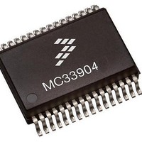
MCZ33904B3EK Freescale Semiconductor, MCZ33904B3EK Datasheet - Page 49

MCZ33904B3EK
Manufacturer Part Number
MCZ33904B3EK
Description
IC SBC CAN HS 3.3V 32SOIC
Manufacturer
Freescale Semiconductor
Type
High Speed CAN Interfacer
Specifications of MCZ33904B3EK
Operating Supply Voltage
3.3 V
Supply Current
2 mA
Package / Case
SOIC-32
Mounting Style
SMD/SMT
Product
CAN
Lead Free Status / RoHS Status
Lead free / RoHS Compliant
Available stocks
Company
Part Number
Manufacturer
Quantity
Price
Company:
Part Number:
MCZ33904B3EKR2
Manufacturer:
FREESCA
Quantity:
4 975
interface. It consist in a low side driver between CANL and
gnd, and high side driver from CANH to 5 V-CAN. Two
differential receivers are connected between CANH and
CANL, to detect bus state and to wake up from CAN Sleep
CAN INTERFACE SUPPLY
The CAN interface also has a supply pass from the battery
line, through the VSUP2 pin. This pass is used in CAN Sleep
mode to allow wake-up detection.
the CAN interface current is sourced from the 5 V-CAN pin.
During CAN Low Power mode, the current is sourced from
the VSUP2 pin.
TXD/RXD MODE
are ON. In this mode, the CAN lines are controlled by the TXD
pin level, and the CAN bus state is reported on the RXD pin.
Analog Integrated Circuit Device Data
Freescale Semiconductor
The figure below is a high level schematic of the CAN
The supply voltage for the CAN driver is the 5 V-CAN pin.
During CAN communication (transmission and reception),
In TxD/RxD mode, both the CAN driver and the receiver
5 V-CAN
RXD
TXD
SPI & State machine
SPI & State machine
5 V-CAN
SPI & State machine
Figure 30. CAN Interface Block Diagram
CAN INTERFACE DESCRIPTION
CAN INTERFACE
2.5 V
Thermal
Failure Detection
& Management
Differential
Detection
Pattern
Receiver
Driver
mode. An internal 2.5 V reference provide the 2.5 V
recessive level via the matched R
can be switched to GND in CAN Sleep mode. A dedicated
split buffer provide a low-impedance 2.5 V to the Split pin, for
recessive level stabilization.
driver and receiver.The SPLIT pin is active and a 2.5 V
biasing is provided on the SPLIT output pin.
RECEIVE ONLY MODE
CAN receiver active. In this mode, the device is only able to
report the CAN state on the RXD pin. The TXD pin has no
effect on CAN bus lines. The 5 V-CAN regulator must be ON.
The SPLIT pin is active and a 2.5 V biasing is provided on the
SPLIT output pin.
OPERATION in TXD/RXD Mode
Normal mode and the TXD pin is recessive.
Driver
The 5 V-CAN regulator must be ON. It supplies the CAN
This mode is used to disable the CAN driver, but leave the
The CAN driver will be enable as soon as the device is in
5 V-CAN
VSUP2
R
R
Wake-up
IN
IN
Receiver
QL
QH
Buffer
CAN INTERFACE DESCRIPTION
IN
CANH
CANL
SPLIT
resistors. The resistors
CAN INTERFACE
33903/4/5
49


