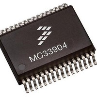
MCZ33904B3EK Freescale Semiconductor, MCZ33904B3EK Datasheet - Page 61

MCZ33904B3EK
Manufacturer Part Number
MCZ33904B3EK
Description
IC SBC CAN HS 3.3V 32SOIC
Manufacturer
Freescale Semiconductor
Type
High Speed CAN Interfacer
Specifications of MCZ33904B3EK
Operating Supply Voltage
3.3 V
Supply Current
2 mA
Package / Case
SOIC-32
Mounting Style
SMD/SMT
Product
CAN
Lead Free Status / RoHS Status
Lead free / RoHS Compliant
Available stocks
Company
Part Number
Manufacturer
Quantity
Price
Company:
Part Number:
MCZ33904B3EKR2
Manufacturer:
FREESCA
Quantity:
4 975
MUX AND RAM REGISTERS
Analog Integrated Circuit Device Data
Freescale Semiconductor
The following tables contain register bit meaning arranged by register address, from address 0_000 to address 1_0100
Table 13. MUX Register
Notes
25.
b7 b6 b5
[b_15 b_14] 0_0000 [P/N]
Bits
000
001
010
011
100
101
110
111
b4
b3
MOSI First Byte [15-8]
0
1
0
1
Condition for default
The MUX register can be written and read only when the 5V-CAN regulator is ON. If the MUX register is written or read while
5V-CAN is OFF, the command is ignored, and the MXU register content is reset to default state (all control bits = 0).
01 00 _ 000 P
Default state
INT 2k - Select device internal 2.0 kohm resistor between AMUX and GND. This resistor allows the measurement of a voltage proportional
V
DD
MUX_2, MUX_1, MUX_0 - Selection of external input signal or internal signal to be measured at MUX-OUT pin
regulator current recopy. Ratio is approx 1/97. Requires an external resistor or selection of Internal 2.0 K (bit 3)
(25)
I/O-att - When I/O-0 (or I/O-1) is selected with b7,b6,b5 = 100 (or 101), b3 selects attenuation or gain
Attenuation is approx 6 for device with V
Attenuation is approx 4 for device with V
Internal 2.0 kohm resistor disable. An external resistor must be connected between AMUX and GND.
DETAIL OF CONTROL BITS AND REGISTER MAPPING
Gain is approx 1.3 for device with V
MUX_2
Gain is approx 2 for device with V
bit 7
0
Voltage at VSENSE pin. Refer to electrical table for attenuation ratio (approx 5)
Voltage at VSUP_1 pin. Refer to electrical table for attenuation ratio (approx 5)
MUX_1
bit 6
All functions disable. No output voltage at MUX-OUT pin
Voltage at I/O-0. Attenuation or gain is selected by bit 3.
Voltage at I/O-1. Attenuation or gain is selected by bit 3.
0
Device internal voltage reference (approx 2.5 V)
Device internal temperature sensor voltage
between I/O-0 (or I/O-1) and MUX-OUT pin
Internal 2.0 kohm resistor enable.
MUX_0
POR, 5 V-CAN off, any mode different from Normal
bit 5
to the V
0
DD
DD
DD
DD
= 5.0 V (Ref to electrical table for exact attenuation value)
= 3.3 V (Ref to electrical table for exact attenuation value)
= 5.0 V (Ref to electrical table for exact gain value)
Description
= 3.3 V (Ref to electrical table for exact gain value)
DD
MOSI Second Byte, bits 7-0
output current.
Int 2K
bit 4
0
DETAIL OF CONTROL BITS AND REGISTER MAPPING
I/O-att
bit 3
0
bit 2
0
0
SERIAL PERIPHERAL INTERFACE
bit 1
0
0
bit 0
0
0
33903/4/5
61


