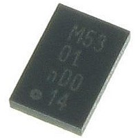
NX3L1T53GD,125 NXP Semiconductors, NX3L1T53GD,125 Datasheet - Page 5

NX3L1T53GD,125
Manufacturer Part Number
NX3L1T53GD,125
Description
IC ANALOG SWITCH SPDT XSON8U
Manufacturer
NXP Semiconductors
Datasheet
1.NX3L1T53GD125.pdf
(24 pages)
Specifications of NX3L1T53GD,125
Number Of Switches
1
Switch Configuration
SPDT
On Resistance (max)
1.6 Ohms
On Time (max)
120 ns
Off Time (max)
90 ns
Off Isolation (typ)
- 90 dB
Supply Voltage (max)
4.3 V
Supply Voltage (min)
1.4 V
Supply Current
690 nA, 800 nA
Maximum Power Dissipation
250 mW
Maximum Operating Temperature
+ 125 C
Mounting Style
SMD/SMT
Package / Case
XSON-8U
Minimum Operating Temperature
- 40 C
Off State Leakage Current (max)
+/- 500 nA
Operating Frequency
60 MHz
Power Dissipation
250 mW
Switch Current (typ)
+/- 350 mA, +/- 500 mA
Lead Free Status / RoHS Status
Lead free / RoHS Compliant
Other names
568-5545-2
NXP Semiconductors
9. Limiting values
Table 5.
In accordance with the Absolute Maximum Rating System (IEC 60134). Voltages are referenced to GND (ground = 0 V).
[1]
[2]
[3]
10. Recommended operating conditions
Table 6.
[1]
[2]
NX3L1T53_4
Product data sheet
Symbol
V
V
V
I
I
I
T
P
Symbol Parameter
V
V
V
T
Δt/ΔV
IK
SK
SW
stg
amb
CC
I
SW
tot
CC
I
SW
The minimum input voltage rating may be exceeded if the input current rating is observed.
The minimum and maximum switch voltage ratings may be exceeded if the switch clamping current rating is observed but may not
exceed 4.6 V.
For XSON8, XSON8U and XQFN8U packages: above 118 °C the value of P
To avoid sinking GND current from terminal Z when switch current flows in terminal Yn, the voltage drop across the bidirectional switch
must not exceed 0.4 V. If the switch current flows into terminal Z, no GND current will flow from terminal Yn. In this case, there is no limit
for the voltage drop across the switch.
Applies to control signal levels.
supply voltage
input voltage
switch voltage
ambient temperature
input transition rise and fall rate V
Limiting values
Recommended operating conditions
Parameter
supply voltage
input voltage
switch voltage
input clamping current
switch clamping current
switch current
storage temperature
total power dissipation
Conditions
select input S and enable input E
V
V
V
source or sink current
V
pulsed at 1 ms duration, < 10 % duty cycle;
peak current
T
amb
I
I
SW
SW
< −0.5 V
< −0.5 V or V
Conditions
select input S and enable
input E
CC
> −0.5 V or V
> −0.5 V or V
= −40 °C to +125 °C
= 1.4 V to 4.3 V
Rev. 04 — 24 March 2010
I
> V
SW
SW
CC
< V
< V
Low-ohmic single-pole double-throw analog switch
+ 0.5 V
CC
CC
+ 0.5 V;
+ 0.5 V;
tot
derates linearly with 7.8 mW/K.
[1]
[2]
Min
1.4
0
0
−40
-
Typ
-
-
-
-
-
[1]
[2]
[3]
Min
−0.5
−0.5
−0.5
−50
-
-
-
−65
-
NX3L1T53
Max
4.3
4.3
V
+125
200
© NXP B.V. 2010. All rights reserved.
CC
Max
+4.6
+4.6
V
-
±50
±350
±500
+150
250
CC
+ 0.5 V
Unit
V
V
V
°C
ns/V
5 of 24
Unit
V
V
mA
mA
mA
mA
°C
mW


