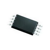
NX3V1T66GW,125 NXP Semiconductors, NX3V1T66GW,125 Datasheet - Page 11

NX3V1T66GW,125
Manufacturer Part Number
NX3V1T66GW,125
Description
IC ANALOG SWITCH SPST UMT5
Manufacturer
NXP Semiconductors
Datasheet
1.NX3V1T66GM132.pdf
(20 pages)
Specifications of NX3V1T66GW,125
Number Of Switches
1
Switch Configuration
SPST
On Resistance (max)
0.8 Ohms
On Time (max)
57 ns
Off Time (max)
90 ns
Off Isolation (typ)
- 90 dB
Supply Voltage (max)
4.3 V
Supply Voltage (min)
1.4 V
Supply Current
690 nA, 800 nA
Maximum Power Dissipation
250 mW
Maximum Operating Temperature
+ 125 C
Mounting Style
SMD/SMT
Package / Case
TSSOP-5
Minimum Operating Temperature
- 40 C
Off State Leakage Current (max)
+/- 500 nA
Operating Frequency
25 MHz
Power Dissipation
250 mW
Switch Current (typ)
+/- 500 mA, +/- 750 mA
Lead Free Status / RoHS Status
Lead free / RoHS Compliant
Other names
568-5568-2
NXP Semiconductors
Table 12.
At recommended operating conditions; voltages are referenced to GND (ground = 0 V); V
specified); t
[1]
NX3V1T66
Product data sheet
Symbol Parameter
THD
f
V
Q
(3dB)
Fig 17. Test circuit for measuring total harmonic distortion
iso
ct
inj
f
i
is biased at 0.5V
total harmonic
distortion
3 dB frequency
response
isolation (OFF-state)
crosstalk voltage
charge injection
r
Additional dynamic characteristics
= t
f
12.2 Additional dynamic characteristics
12.3 Test circuits
2.5 ns; T
CC
.
amb
= 25
Conditions
f
R
f
between digital inputs and switch;
f
f
R
i
i
i
i
C.
= 20 Hz to 20 kHz; R
L
= 100 kHz; R
= 1 MHz; C
= 1 MHz; C
gen
V
V
V
V
V
V
V
V
V
V
V
V
V
V
= 50 ; see
CC
CC
CC
CC
CC
CC
CC
CC
CC
CC
CC
CC
CC
CC
= 0 ; see
= 1.4 V; V
= 1.65 V; V
= 2.3 V; V
= 2.7 V; V
= 4.3 V; V
= 1.4 V to 4.3 V
= 1.4 V to 4.3 V
= 1.4 V to 3.6 V
= 3.6 V to 4.3 V
= 1.5 V
= 1.8 V
= 2.5 V
= 3.3 V
= 4.3 V
All information provided in this document is subject to legal disclaimers.
V
IH
f i
L
L
Rev. 6 — 21 December 2010
= 50 pF; R
= 0.1 nF; R
L
Y/Z
Figure 18
Figure 21
= 50 ; see
I
I
I
I
E
= 1 V (p-p)
= 1.5 V (p-p)
= 2 V (p-p)
= 2 V (p-p)
I
= 1.2 V (p-p)
L
V
= 32 ; see
CC
L
L
= 50 ; see
= 1 M; V
Low-ohmic single-pole single-throw analog switch
Figure 19
Z/Y
0.5V
Figure 17
gen
Figure 20
001aah378
CC
R L
= 0 V;
D
I
= GND or V
[1]
[1]
[1]
Min
-
-
-
-
-
-
-
-
-
-
-
-
-
-
NX3V1T66
CC
Typ
0.05
0.03
0.01
0.01
0.01
© NXP B.V. 2010. All rights reserved.
90
0.3
0.5
6.5
6.5
6.5
6.5
25
12
(unless otherwise
Max
-
-
-
-
-
-
-
-
-
-
-
-
-
-
11 of 20
Unit
MHz
pC
pC
pC
pC
pC
dB
%
%
%
%
%
V
V


