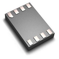
74LVC2G38GD,125 NXP Semiconductors, 74LVC2G38GD,125 Datasheet - Page 7

74LVC2G38GD,125
Manufacturer Part Number
74LVC2G38GD,125
Description
IC GATE NAND DUAL 2INP OD XSON8U
Manufacturer
NXP Semiconductors
Datasheet
1.74LVC2G38GD125.pdf
(21 pages)
Specifications of 74LVC2G38GD,125
Product
NAND
Logic Family
CMOS
Number Of Gates
2
Propagation Delay Time
4.2 ns, 5.2 ns, 5.5 ns, 6 ns, 10.8 ns
Supply Voltage (max)
5.5 V
Maximum Operating Temperature
+ 125 C
Mounting Style
SMD/SMT
Package / Case
XSON-8U
Minimum Operating Temperature
- 40 C
Lead Free Status / RoHS Status
Lead free / RoHS Compliant
Other names
568-5474-2
NXP Semiconductors
Table 7.
At recommended operating conditions; voltages are referenced to GND (ground = 0 V).
[1]
11. Dynamic characteristics
Table 8.
Voltages are referenced to GND (ground 0 V); for test circuit see
[1]
[2]
74LVC2G38
Product data sheet
Symbol Parameter
I
I
I
ΔI
Symbol Parameter
t
t
C
I
OFF
CC
PZL
PLZ
PD
CC
All typical values are measured at T
Typical values are measured at nominal V
C
P
f
f
C
V
N = number of inputs switching;
Σ(C
i
o
D
CC
PD
= input frequency in MHz;
L
= output frequency in MHz;
= output load capacitance in pF;
= C
L
is used to determine the dynamic power dissipation (P
= supply voltage in V;
× V
input leakage current
power-off leakage current V
supply current
additional supply current
OFF-state to LOW
propagation delay
LOW to OFF-state
propagation delay
power dissipation
capacitance
PD
Static characteristics
Dynamic characteristics
CC
× V
2
× f
CC
o
2
) = sum of outputs.
× f
i
× N + Σ(C
Conditions
nA, nB to nY; see
nA, nB to nY; see
per gate; V
L
V
V
V
V
V
V
V
V
V
V
× V
CC
CC
CC
CC
CC
CC
CC
CC
CC
CC
…continued
CC
amb
= 1.65 V to 1.95 V
= 2.3 V to 2.7 V
= 2.7 V
= 3.0 V to 3.6 V
= 4.5 V to 5.5 V
= 1.65 V to 1.95 V
= 2.3 V to 2.7 V
= 2.7 V
= 3.0 V to 3.6 V
= 4.5 V to 5.5 V
Conditions
V
V
V
per pin; V
V
2
I
I
I
CC
CC
× f
= 25 °C.
= 5.5 V or GND; V
or V
= 5.5 V or GND;
I
CC
o
All information provided in this document is subject to legal disclaimers.
= 1.65 V to 5.5 V; I
= 2.3 V to 5.5 V
= GND to V
) where:
and at T
O
= 5.5 V; V
I
Figure 8
Figure 8
= V
Rev. 8 — 4 November 2010
amb
CC
CC
− 0.6 V; I
= 25 °C.
CC
D
in μW).
CC
= 0 V
O
= 0 V to 5.5 V
[2]
= 0 A
O
Figure
= 0 A;
Min
1.2
0.7
0.7
0.7
0.5
1.2
0.7
0.7
0.7
0.5
-
−40 °C to +85 °C
9.
Typ
3.0
1.8
2.5
2.1
1.5
3.0
1.8
2.5
2.1
1.5
5
Dual 2-input NAND gate; open drain
[1]
Min
-
-
-
-
Max
8.6
4.8
4.4
4.1
3.3
8.6
4.8
4.4
4.1
3.3
-
Typ
-
-
-
-
−40 °C to +125 °C Unit
74LVC2G38
Min
1.2
0.7
0.7
0.7
0.5
1.2
0.7
0.7
0.7
0.5
-
Max
±20
±20
40
5000
© NXP B.V. 2010. All rights reserved.
Max
10.8
10.8
6.0
5.5
5.2
4.2
6.0
5.5
5.2
4.2
-
Unit
μA
μA
μA
μA
ns
ns
ns
ns
ns
ns
ns
ns
ns
ns
pF
7 of 21


