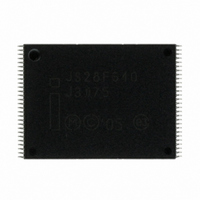
JS28F640J3D75E NUMONYX, JS28F640J3D75E Datasheet - Page 21

JS28F640J3D75E
Manufacturer Part Number
JS28F640J3D75E
Description
IC FLASH 64MBIT 75NS 56TSOP
Manufacturer
NUMONYX
Datasheet
1.PC28F640J3D75E.pdf
(68 pages)
Specifications of JS28F640J3D75E
Format - Memory
FLASH
Memory Type
FLASH
Memory Size
64M (8Mx8, 4Mx16)
Speed
75ns
Interface
Parallel
Voltage - Supply
2.7 V ~ 3.6 V
Operating Temperature
-40°C ~ 85°C
Package / Case
56-TSOP
Lead Free Status / RoHS Status
Lead free / RoHS Compliant
Other names
876760
876760
JS28F640J3D75 S L8YQ
876760
JS28F640J3D75 S L8YQ
Available stocks
Company
Part Number
Manufacturer
Quantity
Price
Part Number:
JS28F640J3D75E
Manufacturer:
MUMONYS
Quantity:
20 000
Company:
Part Number:
JS28F640J3D75ES
Manufacturer:
NS
Quantity:
440
Part Number:
JS28F640J3D75ES
Manufacturer:
INTEL
Quantity:
20 000
Numonyx™ Embedded Flash Memory (J3 v. D)
6.0
6.1
Table 7:
November 2007
308551-05
V
Notes:
1.
2.
3.
4.
5.
Symbol
CC
I
I
I
I
I
I
CCWS
CCES
I
CCW
CCD
I
CCS
CCE
LO
LI
Page Mode Read Current
All currents are in RMS unless otherwise noted. These currents are valid for all product versions (packages and
speeds). Contact Numonyx’s Application Support Hotline or your local sales office for information about typical
specifications.
Includes STS.
CMOS inputs are either V
Sampled, not 100% tested.
I
mode, the device’s current draw is I
CCWS
Input and V
Output Leakage Current
V
V
V
Lock-Bit Current
V
Clear Block Lock-Bits
Current
V
Suspend or Block
Erase Suspend
Current
CC
CC
CC
CC
CC
I
DC Current Characteristics
CCR
and I
Standby Current
Power-Down Current
Program or Set
Block Erase or
Program
Electrical Characteristics
DC Current Specifications
CCES
PEN
V
V
CCQ
Parameter
are specified with the device selected. If the device is read or written while in erase suspend
CC
Load Current
CC
32, 64, 128 Mbit
32, 64, 128 Mbit
8-Word Page
± 0.2 V or GND ± 0.2 V. TTL inputs are either V
256 Mbit
256 Mbit
4-Word
Page
CCR
and I
CCWS
0.71
1.42
Typ
100
50
50
15
24
10
30
35
40
35
40
2.7 - 3.6V
2.7 - 3.6V
.
Max
120
240
120
±10
20
29
15
54
60
70
70
80
10
±1
2
4
Unit
mA
mA
mA
mA
mA
mA
mA
mA
mA
mA
μA
μA
μA
μA
V
V
V
V
CMOS Inputs, V
VccqMax
Device is disabled RP# = V
TTL Inputs, V
Vccq = VccqMax
Device is disabled, RP# = V
RP# = GND ± 0.2 V, I
CMOS Inputs, V
Max
Device is enabled f = 5 MHz, I
CMOS Inputs,V
Max
Device is enabled f = 33 MHz, I
CMOS Inputs, V
Max using standard 8 word page mode
reads.
Device is enabled f = 5 MHz, I
CMOS Inputs,V
Max using standard 8 word page mode
reads.
Device is enabled f = 33 MHz, I
CMOS Inputs, V
TTL Inputs, V
CMOS Inputs, V
TTL Inputs, V
Device is enabled
CC
IN
CC
IN
= V
= V
= V
= V
CC
CCQ
CCQ
CC
IL
Max; V
Max; V
or V
or V
or V
Test Conditions
CC
PEN
PEN
IH
CC
CC
SS
SS
CC
CC
CC
PEN
PEN
= V
.
CCQ
= V
= V
CCQ
= V
= V
= V
= V
= V
= V
= V
CC
CC
CC
= V
CC
CC
= V
OUT
CC
CC
CC
Max,
CC
CC
Max, V
Max, V
CCQ
Max, V
Max, V
Max; Vccq =
CCQ
(STS) = 0 mA
CCQ
IH
Max
Max
OUT
OUT
± 0.2 V
CCQ
CCQ
OUT
OUT
CCQ
CCQ
= 0 mA
= 0 mA
= V
= 0 mA
= V
= 0 mA
= V
= V
CCQ
CCQ
CCQ
CCQ
Datasheet
Notes
1,2,3
1,3
1,4
1,4
1,5
1
1
21


