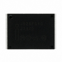
JS28F640J3D75E NUMONYX, JS28F640J3D75E Datasheet - Page 63

JS28F640J3D75E
Manufacturer Part Number
JS28F640J3D75E
Description
IC FLASH 64MBIT 75NS 56TSOP
Manufacturer
NUMONYX
Datasheet
1.PC28F640J3D75E.pdf
(68 pages)
Specifications of JS28F640J3D75E
Format - Memory
FLASH
Memory Type
FLASH
Memory Size
64M (8Mx8, 4Mx16)
Speed
75ns
Interface
Parallel
Voltage - Supply
2.7 V ~ 3.6 V
Operating Temperature
-40°C ~ 85°C
Package / Case
56-TSOP
Lead Free Status / RoHS Status
Lead free / RoHS Compliant
Other names
876760
876760
JS28F640J3D75 S L8YQ
876760
JS28F640J3D75 S L8YQ
Available stocks
Company
Part Number
Manufacturer
Quantity
Price
Part Number:
JS28F640J3D75E
Manufacturer:
MUMONYS
Quantity:
20 000
Company:
Part Number:
JS28F640J3D75ES
Manufacturer:
NS
Quantity:
440
Part Number:
JS28F640J3D75ES
Manufacturer:
INTEL
Quantity:
20 000
Numonyx™ Embedded Flash Memory (J3 v. D)
Table 40: Primary Vendor-Specific Extended Query (Sheet 2 of 2)
November 2007
308551-05
Note:
1.
2.
Offset
P = 31h
(P+D)h
(P+5)h
(P+6)h
(P+7)h
(P+8)h
(P+9)h
(P+A)h
(P+B)h
(P+C)h
(1)
Future devices may not support the described “Legacy Lock/Unlock” function. Thus bit 3 would have a value of “0.”
Setting this bit, will lead to the extension of the CFI table. Please refer to
Length
4
1
2
1
1
Optional feature and command support (1=yes, 0=no)
“1” then another 31 bit field of optional features follows at
the end of the bit-30 field.
bit 0 Chip erase supported
bit 1 Suspend erase supported
bit 2 Suspend program supported
bit 3 Legacy lock/unlock supported
bit 4 Queued erase supported
bit 5 Instant Individual block locking supported
bit 6 Protection bits supported
bit 7 Page-mode read supported
bit 8 Synchronous read supported
bit9 Simultaneous Operation Supported
bit 30 CFI Link(s) to follow (32, 64, 128- Mb)
bit 30 CFI Link(s) to follow (256 Mb)
bit 31 Another “Optional Feature” field to follow
Supported functions after suspend: read Array, Status, Query
bit 0 Program supported after erase suspend
Block Status Register mask
bits 2–15 are Reserved; undefined bits are “0”
bit 0 Block Lock-Bit Status register active
bit 1 Block Lock-Down Bit Status active
V
V
Undefined bits are “0.” If bit 31 is
CC
PP
Other supported operations are:
bits 1–7 reserved; undefined bits are “0”
bits 0–3 BCD value in 100 mV
bits 4–7 BCD value in volts
bits 0–3 BCD value in 100 mV
bits 4–7 HEX value in volts
optimum program/erase supply voltage
logic supply highest performance program/erase voltage
(Optional Flash Features and Commands)
Description
Table 43
.
Add.
3A:
3B:
3C:
3D:
36:
37:
38:
39:
3E:
bit 30 = 0
bit 30 = 0
bit 30 = 1
bit 31 = 0
bit 3 = 1
bit 0 = 0
bit 1 = 1
bit 2 = 1
bit 4 = 0
bit 5 = 0
bit 6 = 1
bit 7 = 1
bit 8 = 0
bit 9 = 0
bit 0 = 1
bit 0 = 1
bit 1 = 0
(1)
Code
--CE
Hex
--00
--00
--00
--01
--01
--00
--33
--00
Datasheet
Value
Yes
3.3 V
0.0 V
Yes
Yes
Yes
Yes
Yes
Yes
Yes
No
No
No
No
No
No
No
No
No
(1)
63


