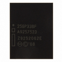
RC28F256P33BFA NUMONYX, RC28F256P33BFA Datasheet - Page 65

RC28F256P33BFA
Manufacturer Part Number
RC28F256P33BFA
Description
IC FLASH 256MBIT 95NS 64EZBGA
Manufacturer
NUMONYX
Series
Axcell™r
Specifications of RC28F256P33BFA
Format - Memory
FLASH
Memory Type
FLASH
Memory Size
256M (16Mx16)
Speed
95ns
Interface
Parallel
Voltage - Supply
2.3 V ~ 3.6 V
Operating Temperature
-40°C ~ 85°C
Package / Case
64-EZBGA
Cell Type
NOR
Density
256Mb
Interface Type
Parallel/Serial
Boot Type
Bottom
Address Bus
25b
Operating Supply Voltage (typ)
2.5/3/3.3V
Operating Temp Range
-40C to 85C
Package Type
EZBGA
Sync/async
Async/Sync
Operating Temperature Classification
Industrial
Operating Supply Voltage (min)
2.3V
Operating Supply Voltage (max)
3.6V
Word Size
16b
Number Of Words
32M
Supply Current
50mA
Mounting
Surface Mount
Pin Count
64
Lead Free Status / RoHS Status
Contains lead / RoHS non-compliant
Other names
898897
898897
RC28F256P33BF 898897
898897
RC28F256P33BF 898897
Available stocks
Company
Part Number
Manufacturer
Quantity
Price
Company:
Part Number:
RC28F256P33BFA
Manufacturer:
Micron Technology Inc
Quantity:
10 000
P33-65nm
A.1.5
Table 34: Primary Vendor-Specific Extended Query
Datasheet
65
P = 10Ah
Offset
A ddress
(P+A)h
(P+0)h
(P+1)h
(P+2)h
(P+3)h
(P+4)h
(P+5)h
(P+6)h
(P+7)h
(P+8)h
(P+9)h
(P+B)h
(P+C)h
(P+D)h
112:
(1)
Length
3
1
1
4
1
2
1
1
--00
–B
–-
Numonyx-Specific Extended Query Table
Discrete
Primary extended query table
Major version number, ASCII
Minor version number, ASCII
Optional feature and command support (1=yes, 0=no)
Block status register mask
Supported functions after suspend: read Array, Status, Query
V
V
CC
PP
Other supported operations are:
bits 1–7 reserved; undefined bits are “0”
bits 0–3 BCD value in 100 mV
bits 4–7 BCD value in volts
bits 0–3 BCD value in 100 mV
bits 4–7 HEX value in volts
logic supply highest performance program/erase voltage
optimum program/erase supply voltage
--00
Unique ASCII string “PRI“
bits 10–31 are reserved; undefined bits are “0.” If bit 31 is
“1” then another 31 bit field of Optional features follows at
the end of the bit–30 field.
bit 0 Chip erase supported
bit 1 Suspend erase supported
bit 2 Suspend program supported
bit 3 Legacy lock/unlock supported
bit 4 Queued erase supported
bit 5 Instant individual block locking supported
bit 6 Protection bits supported
bit 7 Pagemode read supported
bit 8 Synchronous read supported
bit 9 Simultaneous operations supported
bit 10 Extended Flash Array Blocks supported
bit 11 Permanent Block Locking of up to Full Main Array supported
bit 12 Permanent Block Locking of up to Partial Main Array supported
bit 30 CFI Link(s) to follow
bit 31 Another "Optional Features" field to follow
bit 0 Program supported after erase suspend
bits 2–15 are Reserved; undefined bits are “0”
bit 0 Block Lock-Bit Status register active
bit 1 Block Lock-Dow n Bit Status active
bit 4 EFA Block Lock-Bit Status register active
bit 5 EFA Block Lock-Dow n Bit Status active
–T
–-
die 1 (B)
--40
(Optional flash features and com m ands)
–B
die 2 (T)
--00
512-Mbit
Description
die 1 (T)
--40
–T
die 2 (B)
--00
Order Number:320003-09
Add.
10B:
10C:
10D:
10E:
10F:
110:
111:
112:
113:
114:
115:
116:
117:
10A
bit 10 = 0
bit 11 = 1
bit 12 = 0
bit 30 = 1
bit 31 = 0
bit 0 = 0
bit 1 = 1
bit 2 = 1
bit 3 = 0
bit 4 = 0
bit 5 = 1
bit 6 = 1
bit 7 = 1
bit 8 = 1
bit 9 = 0
bit 0 = 1
bit 0 = 1
bit 1 = 1
bit 4 = 0
bit 5 = 0
Code
Hex
--50
--52
--49
--31
--35
--E6
--09
--00
--40
--01
--03
--00
--18
--90
Mar 2010
Value
1.8V
9.0V
Yes
Yes
Yes
Yes
Yes
Yes
Yes
Yes
Yes
Yes
Yes
"R"
"P"
"1"
"5"
No
No
No
No
No
No
No
No
No
"I"


