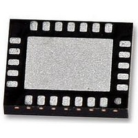
LM25066APSQE/NOPB National Semiconductor, LM25066APSQE/NOPB Datasheet - Page 13

LM25066APSQE/NOPB
Manufacturer Part Number
LM25066APSQE/NOPB
Description
IC CTLR PM HOTSWAP 24-LLP
Manufacturer
National Semiconductor
Series
PowerWise®r
Specifications of LM25066APSQE/NOPB
Applications
Base Station-Networking Line Cards, Servers
Current - Supply
5.8mA
Voltage - Supply
2.9 V ~ 17 V
Operating Temperature
-40°C ~ 85°C
Mounting Type
*
Package / Case
*
Input Voltage
17V
Internal Switch
No
Supply Voltage Range
2.9V To 5.5V
Rohs Compliant
Yes
Digital Ic Case Style
LLP
No. Of Pins
24
Lead Free Status / RoHS Status
Lead free / RoHS Compliant
Other names
LM25066APSQE/NOPBTR
Power Up Sequence
The VIN operating range of the LM25066A is +2.9V to +17V
with transient capability to +24V. Referring to
Figure
N-channel MOSFET (Q
pull-down current at the GATE pin. The strong pull-down cur-
rent at the GATE pin prevents an inadvertent turn-on as the
MOSFET’s gate-to-drain (Miller) capacitance is charged. Ad-
ditionally, the TIMER pin is initially held at ground. When the
VIN voltage reaches the POR threshold, the insertion time
begins. During the insertion time, the capacitor at the TIMER
pin (C
off by a 2 mA pull-down current at the GATE pin regardless
of the input voltage. The insertion time delay allows ringing
and transients at VIN to settle before Q
sertion time ends when the TIMER pin voltage reaches 1.7V.
C
current. The GATE pin then switches on Q
voltage, V
the UVLO threshold at the end of the insertion time, Q
es on at that time. The GATE pin charge pump sources 22 µA
to charge the gate capacitance of Q
at the GATE pin with respect to ground is limited by an internal
18.8V zener diode.
T
is then quickly discharged by an internal 1.9 mA pull-down
T
2, as the voltage at VIN initially increases, the external
) is charged by a 5.5 µA current source and Q
SYS
, exceeds the UVLO threshold. If V
1
) is held off by an internal 190 mA
1
. The maximum voltage
1
is enabled. The in-
1
FIGURE 1. Typical Application Circuit
when the input
Figure 1
SYS
is above
1
1
switch-
is held
and
13
As the voltage at the OUT pin increases, the LM25066A mon-
itors the drain current and power dissipation of MOSFET Q
Inrush current limiting and/or power limiting circuits actively
control the current delivered to the load. During the inrush
limiting interval (t
current source charges C
input current reduce below their respective limiting thresholds
before the TIMER pin reaches 1.7V, the 90 µA current source
is switched off and C
current sink (t
the voltage at FB exceeds its rising threshold of 1.167V.
If the TIMER pin voltage reaches 1.7V before inrush current
limiting or power limiting ceases during t
and Q
a complete description of the fault mode.
The LM25066A will pull the SMBA pin low after the input volt-
age has exceeded its POR threshold to indicate that the
volatile memory and device settings are in their default state.
The CONFIG_PRESET bit within the STATUS_MFR_SPE-
CIFIC register (80h) indicates default configuration of warning
thresholds and device operation and will remain set until a
CLEAR_FAULTS command is received.
1
is turned off. See the Fault Timer & Restart section for
3
in
2
Figure
in
Figure
T
is discharged by the internal 2.8 µA
2). The PGD pin switches high when
T
. If Q
2), an internal 90 µA fault timer
1
’s power dissipation and the
2
, a fault is declared
www.national.com
30146011
1
.


