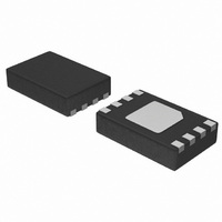
CAT34TS02VP2GT4B ON Semiconductor, CAT34TS02VP2GT4B Datasheet - Page 2

CAT34TS02VP2GT4B
Manufacturer Part Number
CAT34TS02VP2GT4B
Description
IC TEMP SENSOR 2KB MEM 8-TDFN
Manufacturer
ON Semiconductor
Datasheet
1.CAT34TS02VP2GT4A.pdf
(22 pages)
Specifications of CAT34TS02VP2GT4B
Function
Temp Monitoring System (Sensor)
Topology
ADC (Sigma Delta), Comparator, Register Bank
Sensor Type
Internal
Sensing Temperature
-40°C ~ 125°C
Output Type
I²C™, SPI™
Output Alarm
Yes
Output Fan
No
Voltage - Supply
2.97 V ~ 3.63 V
Operating Temperature
-40°C ~ 125°C
Mounting Type
Surface Mount
Package / Case
8-WFDFN Exposed Pad
Digital Output - Bus Interface
I2C, SMBus
Digital Output - Number Of Bits
12 bit
Supply Voltage (min)
3.3 V
Description/function
Digital Output Temperature Sensor with On-board SPD EEPROM
Maximum Operating Temperature
+ 130 C
Minimum Operating Temperature
- 45 C
Supply Current
500 uA
Lead Free Status / RoHS Status
Lead free / RoHS Compliant
Available stocks
Company
Part Number
Manufacturer
Quantity
Price
Company:
Part Number:
CAT34TS02VP2GT4B
Manufacturer:
ON Semiconductor
Quantity:
2 900
Part Number:
CAT34TS02VP2GT4B
Manufacturer:
ON/安森美
Quantity:
20 000
CAT34TS02
Absolute Maximum Ratings
RELIABILITY CHARACTERISTICS
TEMPERATURE CHARACTERISTICS
V
D.C. OPERATING CHARACTERISTICS
V
Notes:
(1) Stresses above those listed under “Absolute Maximum Ratings” may cause permanent damage to the device. These are stress ratings
(2) The DC input voltage on any pin should not be lower than -0.5 V or higher than V
(3) Power Dissipation is defined as P
(4) Page Mode, V
Doc. No. MD-1129 Rev. H
Parameter
Temperature Reading Error
Class B, JC42.4 compliant
ADC Resolution
Temperature Resolution
Conversion Time
Thermal Resistance
Parameter
Operating Temperature
Storage Temperature
Voltage on any pin (except A
Voltage on pin A
CC
CC
Symbol
Symbol
N
only, and functional operation of the device at these or any other conditions outside of those listed in the operational sections of this
specification is not implied. Exposure to any absolute maximum rating for extended periods may affect device performance and reliability.
RSWP command execution. SCL and SDA inputs can be raised to the maximum limit, irrespective of V
resistance value refers to the case of a package being used on a standard 2-layer PCB.
I
V
V
= 3.3 V ± 10%, T
= 3.3 V ± 10%, T
SHDN
I
T
END
V
I
V
LKG
CC
OL1
OL2
DR
IH
IL
(4)
Parameter
Endurance (EEPROM)
Data Retention (EEPROM)
Parameter
Supply Current
Standby Current
I/O Pin Leakage Current
Input Low Voltage
Input High Voltage
Output Low Voltage
Output Low Voltage
CC
= 3.3 V, 25°C
0
with respect to Ground
A
(3)
A
= −40°C to +125°C, unless otherwise specified
= −40°C to +125°C, unless otherwise specified
θ
JA
(1)
0
J
) with respect to Ground
= (T
J
(3)
− T
Test Conditions/Comments
+75°C ≤ T
+40°C ≤ T
-40°C ≤ T
Junction-to-Ambient (Still Air)
A
)/θ
JA
Test Conditions/Comments
TS active, SPD and Bus idle
EEPROM Write, TS shut-down
TS shut-down; SPD and Bus idle
Pin at GND or V
I
I
OL
OL
, where T
= 3 mA, V
= 1 mA, V
A
A
A
≤ +125°C, sensing range
≤ +95°C, active range
≤ +125°C, monitor range
J
is the junction temperature and T
(2)
CC
CC
2
> 2.7 V
< 2.7 V
CC
CC
+ 0.5 V. The A
1,000,000
A
Min
100
is the ambient temperature. The thermal
0.7 x V
Min
-0.5
0
Characteristics subject to change without notice
CC
pin can be raised to a HV level for
.
-0.5 to +10.5
-45 to +130
-65 to +150
-0.5 to +6.5
CC
Rating
© 2010 SCILLC. All rights reserved.
V
0.3 x V
0.0625
CC
Max
±1.0
±2.0
±3.0
Max
100
500
500
Write Cycles
0.4
0.2
12
92
10
2
+ 0.5
Years
Units
CC
Units
ºC/W
Unit
Unit
Bits
ms
°C
°C
μA
μA
μA
μA
°C
°C
°C
°C
V
V
V
V
V
V


