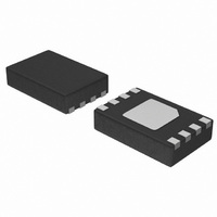
CAT34TS02VP2GT4B ON Semiconductor, CAT34TS02VP2GT4B Datasheet - Page 6

CAT34TS02VP2GT4B
Manufacturer Part Number
CAT34TS02VP2GT4B
Description
IC TEMP SENSOR 2KB MEM 8-TDFN
Manufacturer
ON Semiconductor
Datasheet
1.CAT34TS02VP2GT4A.pdf
(22 pages)
Specifications of CAT34TS02VP2GT4B
Function
Temp Monitoring System (Sensor)
Topology
ADC (Sigma Delta), Comparator, Register Bank
Sensor Type
Internal
Sensing Temperature
-40°C ~ 125°C
Output Type
I²C™, SPI™
Output Alarm
Yes
Output Fan
No
Voltage - Supply
2.97 V ~ 3.63 V
Operating Temperature
-40°C ~ 125°C
Mounting Type
Surface Mount
Package / Case
8-WFDFN Exposed Pad
Digital Output - Bus Interface
I2C, SMBus
Digital Output - Number Of Bits
12 bit
Supply Voltage (min)
3.3 V
Description/function
Digital Output Temperature Sensor with On-board SPD EEPROM
Maximum Operating Temperature
+ 130 C
Minimum Operating Temperature
- 45 C
Supply Current
500 uA
Lead Free Status / RoHS Status
Lead free / RoHS Compliant
Available stocks
Company
Part Number
Manufacturer
Quantity
Price
Company:
Part Number:
CAT34TS02VP2GT4B
Manufacturer:
ON Semiconductor
Quantity:
2 900
Part Number:
CAT34TS02VP2GT4B
Manufacturer:
ON/安森美
Quantity:
20 000
CAT34TS02
PIN DESCRIPTION
SCL: The Serial Clock input pin accepts the Serial
Clock generated by the Master (Host).
SDA: The Serial Data I/O pin receives input data
and transmits data stored in the internal registers. In
transmit mode, this pin is open drain. Data is
acquired on the positive edge, and is delivered on
the negative edge of SCL.
A0, A1 and A2: The Address pins accept the device
address. These pins have on-chip pull-down resistors.
¯¯¯¯¯¯ : The open-drain EVENT
EVENT
programmed to signal over/under temperature limit
conditions.
POWER-ON RESET (POR)
The CAT34TS02 incorporates Power-On Reset
(POR) circuitry which protects the device against
powering up to invalid state. The TS component will
power up into conversion mode after V
the TS POR trigger level and the SPD component
will power up into standby mode after V
the SPD POR trigger level. Both the TS and SPD
components will power down into Reset mode when
V
This bi-directional POR behavior protects the
CAT34TS02 against brown-out failure following a
temporary loss of power. The POR trigger levels are
set below the minimum operating V
DEVICE INTERFACE
The CAT34TS02 supports the Inter-Integrated
Circuit (I
(SMBus)
protocols describe serial communication between
transmitters and receivers sharing a 2-wire data bus.
Data flow is controlled by a Master device, which
generates the serial clock and the START and
STOP conditions. The CAT34TS02 acts as a Slave
device. Master and Slave alternate as transmitter
and receiver. Up to 8 CAT34TS02 devices may be
present on the bus simultaneously, and can be
individually addressed by matching the logic state of
the address inputs A0, A1, and A2.
Doc. No. MD-1129 Rev. H
CC
drops below their respective POR trigger levels.
2
C) and the System Management Bus
data
transmission
¯¯¯¯¯¯ pin can be
protocols.
CC
level.
CC
CC
exceeds
exceeds
These
6
I
The I
and one for data (SDA). The two wires are
connected to the V
Master and Slave devices connect to the bus via
their respective SCL and SDA pins. The transmitting
device pulls down the SDA line to ‘transmit’ a ‘0’ and
releases it to ‘transmit’ a ‘1’.
Data transfer may be initiated only when the bus is
not busy (see A.C. Characteristics).
During data transfer, the SDA line must remain
stable while the SCL line is HIGH. An SDA transition
while SCL is HIGH will be interpreted as a START or
STOP condition (Figure 1).
START
The START condition precedes all commands. It
consists of a HIGH to LOW transition on SDA while
SCL is HIGH. The START acts as a ‘wake-up’ call to
all Slaves. Absent a START, a Slave will not
respond to commands.
STOP
The STOP condition completes all commands. It
consists of a LOW to HIGH transition on SDA while
SCL is HIGH. The STOP tells the Slave that no more
data will be written to or read from the Slave.
DEVICE ADDRESSING
The Master initiates data transfer by creating a START
condition on the bus. The Master then broadcasts an
8-bit serial Slave address. The first 4 bits of the Slave
address (the preamble) select either the Temperature
Sensor (TS) registers (0011) or the EEPROM memory
contents (1010), as shown in Figure 2. The next 3 bits,
A2, A1 and A0, select one of 8 possible Slave devices.
The last bit, R/W ¯ ¯ , specifies whether a Read (1) or
Write (0) operation is being performed
ACKNOWLEDGE
A matching Slave address is acknowledged (ACK)
by the Slave by pulling down the SDA line during the
9
acknowledge all data bytes sent to the bus by the
Master. When the Slave is the transmitter, the
Master will in turn acknowledge data bytes in the 9
clock cycle. The Slave will stop transmitting after the
Master
(NoACK) and then issues a STOP. Bus timing is
illustrated in Figure 4.
2
th
C/SMBUS PROTOCOL
clock cycle (Figure 3). After that, the Slave will
2
C/SMBus uses two ‘wires’, one for clock (SCL)
does
not
CC
respond
supply via pull-up resistors.
Characteristics subject to change without notice
© 2010 SCILLC. All rights reserved.
with
acknowledge
th


