LMK04000BEVAL/NOPB National Semiconductor, LMK04000BEVAL/NOPB Datasheet - Page 48
LMK04000BEVAL/NOPB
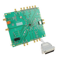
Manufacturer Part Number
LMK04000BEVAL/NOPB
Description
BOARD EVAL PRECISION CLOCK PLL
Manufacturer
National Semiconductor
Series
PowerWise®r
Datasheets
1.LMK04010BISQENOPB.pdf
(54 pages)
2.LMK04002BEVAL.pdf
(56 pages)
3.LMK04002BEVAL.pdf
(38 pages)
Specifications of LMK04000BEVAL/NOPB
Main Purpose
Timing, Clock Conditioner
Embedded
No
Utilized Ic / Part
LMK04000
Primary Attributes
122.88 MHz VCXO
Secondary Attributes
Integrated PLL & VCO
Lead Free Status / RoHS Status
Lead free / RoHS Compliant
Other names
LMK04000BEVAL
LMK04000BEVAL
LMK04000BEVAL


www.national.com
Some LVDS receivers may effectively have internal biasing
on the inputs. In this case, the circuit shown in Figure 11 is
modified by replacing the 50 Ω terminations to V
a single 100 Ω resistor across the input pins of the receiver,
as shown in Figure 12. When using AC coupling with LVDS
outputs, there may be a startup delay observed in the clock
output due to capacitor charging. The previous figures employ
a 0.1 µF capacitor. This value may need to be adjusted to
meet the startup requirements for a particular application.
FIGURE 12. LVDS Termination for a Self-Biased Receiver
LVPECL drivers require a DC path to ground. When AC cou-
pling an LVPECL signal use 120 Ω emitter resistors close to
the LVPECL driver to provide a DC path to ground as shown
in Figure 13. For proper receiver operation, the signal should
be biased to the DC bias level (common mode voltage) spec-
ified by the receiver. The typical DC bias voltage for LVPECL
receivers is 2 V. A Thevenin equivalent circuit (82 Ω resistor
connected to V
with the driver connected to the junction of the 82 Ω and 120
Ω resistors) is a valid termination as shown in Figure 13 for
V
DC coupled example in Figure 10.
FIGURE 13. Differential LVPECL Operation, AC Coupling,
17.8.3 Termination for Single-Ended Operation
A balun can be used with either LVDS or LVPECL drivers to
convert the balanced, differential signal into an unbalanced,
single-ended signal.
FIGURE 11. Differential LVDS Operation, AC Coupling,
Thevenin Equivalent, External Biasing at the Receiver
CC
= 3.3 V. Note this Thevenin circuit is different from the
External Biasing at the Receiver
CC
and a 120 Ω resistor connected to ground
CC
-2 V with
30027182
30027119
30027117
48
It is possible to use an LVPECL driver as one or two separate
800 mVpp signals. When using only one LVPECL driver of a
CLKoutX/CLKoutX* pair, be sure to properly terminated the
unused driver. When DC coupling one of the LMK04000 fam-
ily clock LVPECL drivers, the termination should be 50 Ω to
V
circuit is also a valid termination as shown in Figure 15 for Vcc
= 3.3 V.
When AC coupling an LVPECL driver use a 120 Ω emitter
resistor to provide a DC path to ground and ensure a 50 Ω
termination with the proper DC bias level for the receiver. The
typical DC bias voltage for LVPECL receivers is 2 V (See
Section 17.9.2 Driving CLKin Pins with a Single-Ended
Source). If the companion driver is not used it should be ter-
minated with either a proper AC or DC termination. This latter
example of AC coupling a single-ended LVPECL signal can
be used to measure single-ended LVPECL performance us-
ing a spectrum analyzer or phase noise analyzer. When using
most RF test equipment no DC bias point (0 VDC) is required
for safe and proper operation. The internal 50 Ω termination
of the test equipment correctly terminates the LVPECL driver
being measured as shown in Figure 16.
CC
FIGURE 14. Single-Ended LVPECL Operation, DC
FIGURE 15. Single-Ended LVPECL Operation, DC
FIGURE 16. Single-Ended LVPECL Operation, AC
- 2 V as shown in Figure 14. The Thevenin equivalent
Coupling, Thevenin Equivalent
Coupling
Coupling
30027116
30027114
30027115
Related parts for LMK04000BEVAL/NOPB
Image
Part Number
Description
Manufacturer
Datasheet
Request
R

Part Number:
Description:
Low-noise Clock Jitter Cleaner With Cascaded Plls
Manufacturer:
National Semiconductor Corporation
Datasheet:
Part Number:
Description:
Lmk04000 Family Of Precision Clock Conditioners Low-noise Clock Jitter Cleaner With Cascaded Plls
Manufacturer:
National Semiconductor Corporation
Datasheet:

Part Number:
Description:
National Semiconductor [8-Bit D/A Converter]
Manufacturer:
National Semiconductor
Datasheet:
Part Number:
Description:
National Semiconductor [Media Coprocessor]
Manufacturer:
National Semiconductor
Datasheet:
Part Number:
Description:
Digitally Controlled Tone and Volume Circuit with Stereo Audio Power Amplifier, Microphone Preamp Stage and National 3D Sound
Manufacturer:
National Semiconductor
Datasheet:
Part Number:
Description:
Digitally Controlled Tone and Volume Circuit with Stereo Audio Power Amplifier, Microphone Preamp Stage and National 3D Sound
Manufacturer:
National Semiconductor
Datasheet:
Part Number:
Description:
AC97 Rev 2 Codec with Sample Rate Conversion and National 3D Sound
Manufacturer:
National Semiconductor
Part Number:
Description:
Manufacturer:
National Semiconductor
Datasheet:
Part Number:
Description:
Manufacturer:
National Semiconductor
Datasheet:
Part Number:
Description:
General Purpose, Low Voltage, Low Power, Rail-to-Rail Output Operational Amplifiers
Manufacturer:
National Semiconductor
Datasheet:
Part Number:
Description:
8-bit 20 MSPS flash A/D converter.
Manufacturer:
National Semiconductor
Datasheet:
Part Number:
Description:
Low Noise Quad Operational Amplifier
Manufacturer:
National Semiconductor
Datasheet:
Part Number:
Description:
Quad Differential Line Receivers
Manufacturer:
National Semiconductor
Datasheet:
Part Number:
Description:
Quad High Speed Trapezoidal? Bus Transceiver
Manufacturer:
National Semiconductor
Datasheet: