LMK04000BEVAL/NOPB National Semiconductor, LMK04000BEVAL/NOPB Datasheet - Page 7
LMK04000BEVAL/NOPB
Manufacturer Part Number
LMK04000BEVAL/NOPB
Description
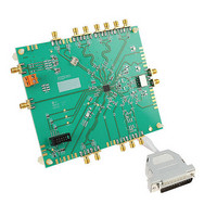
BOARD EVAL PRECISION CLOCK PLL
Manufacturer
National Semiconductor
Series
PowerWise®r
Datasheets
1.LMK04010BISQENOPB.pdf
(54 pages)
2.LMK04002BEVAL.pdf
(56 pages)
3.LMK04002BEVAL.pdf
(38 pages)
Specifications of LMK04000BEVAL/NOPB
Main Purpose
Timing, Clock Conditioner
Embedded
No
Utilized Ic / Part
LMK04000
Primary Attributes
122.88 MHz VCXO
Secondary Attributes
Integrated PLL & VCO
Lead Free Status / RoHS Status
Lead free / RoHS Compliant
Other names
LMK04000BEVAL
LMK04000BEVAL
LMK04000BEVAL


6.0 Pin Descriptions
Pin Number
10
11
12
13
14
15
16
17
18
19
20
21
22
23
24
25
26
27
28
29
30
31
32
33
34
35
36
37
38
39
40
1
2
3
4
5
6
7
8
9
CLKin0_LOS
CLKin1_LOS
DATAuWire
CLKuWire
DLD_BYP
LDObyp1
LDObyp2
CLKout0*
CLKout1*
Name(s)
LEuWire
CLKout0
CLKout1
CLKin0*
CLKin1*
CLKin0
CPout1
CLKin1
OSCin*
CPout2
SYNC*
OSCin
V
V
V
GND
V
V
GOE
V
GND
V
V
V
V
V
V
Fout
Bias
NC
CC
CC
CC
LD
CC
CC
CC
CC
CC
CC
CC
CC
CC
10
11
12
1
2
3
4
5
6
7
8
9
I/O
O
O
O
O
O
O
O
O
O
O
I
I
I
I
I
I
I
I
I
I
I
I
LVPECL/LVCMOS
LVPECL/LVCMOS
LVDS/LVPECL
LVDS/LVPECL
LVCMOS
LVCMOS
CMOS
CMOS
CMOS
CMOS
CMOS
CMOS
ANLG
ANLG
ANLG
ANLG
ANLG
ANLG
ANLG
ANLG
ANLG
ANLG
ANLG
ANLG
ANLG
Type
PWR
PWR
PWR
PWR
PWR
PWR
PWR
PWR
PWR
PWR
PWR
PWR
GND
GND
7
Description
Ground (For Fout Buffer)
VCO Frequency Output Port
Power Supply for VCO Output Buffer
Microwire Clock Input
Microwire Data Input
Microwire Latch Enable Input
No Connection
Power Supply for VCO
LDO Bypass, bypassed to ground with 10 µF and 0.1
µF capacitor
LDO Bypass, bypassed to ground with a 0.1 µF
capacitor
Global Output Enable
Lock Detect and PLL multiplexer Output
Power Supply for CLKout0
Clock Channel 0 Output
Clock Channel 0* Output
DLD Bypass, bypassed to ground with a 0.1 µF
capacitor
Ground (Digital)
Power Supply for Digital
Power Supply for CLKin buffers and PLL1 R-divider
Reference Clock Input Port for PLL1 - AC or DC
Coupled (Note 2)
Reference Clock Input Port for PLL1 (complimentary)
- AC or DC Coupled (Note 2)
Power Supply for PLL1 Phase Detector and Charge
Pump
Charge Pump1 Output
Power Supply for PLL1 N-Divider
Reference Clock Input Port for PLL1 - AC or DC
Coupled (Note 2)
Reference Clock Input Port for PLL1 (complimentary)
- AC or DC Coupled (Note 2)
Global Clock Output Synchronization
Reference oscillator Input for PLL2 - AC Coupled
Reference oscillator Input for PLL2 - AC Coupled
Power Supply for OSCin Buffer and PLL2 R-Divider
Power Supply for PLL2 Phase Detector and Charge
Pump
Charge Pump2 Output
Power Supply for VCO Divider and PLL2 N-Divider
Status of CLKin0 reference clock input
Status of CLKin1 reference clock input
Bias Bypass. AC coupled with 1 µF capacitor to Vcc1
Power Supply for CLKout1
Clock Channel 1 Output
Clock Channel 1* Output
Power Supply for CLKout2
www.national.com
Related parts for LMK04000BEVAL/NOPB
Image
Part Number
Description
Manufacturer
Datasheet
Request
R

Part Number:
Description:
Low-noise Clock Jitter Cleaner With Cascaded Plls
Manufacturer:
National Semiconductor Corporation
Datasheet:
Part Number:
Description:
Lmk04000 Family Of Precision Clock Conditioners Low-noise Clock Jitter Cleaner With Cascaded Plls
Manufacturer:
National Semiconductor Corporation
Datasheet:

Part Number:
Description:
National Semiconductor [8-Bit D/A Converter]
Manufacturer:
National Semiconductor
Datasheet:
Part Number:
Description:
National Semiconductor [Media Coprocessor]
Manufacturer:
National Semiconductor
Datasheet:
Part Number:
Description:
Digitally Controlled Tone and Volume Circuit with Stereo Audio Power Amplifier, Microphone Preamp Stage and National 3D Sound
Manufacturer:
National Semiconductor
Datasheet:
Part Number:
Description:
Digitally Controlled Tone and Volume Circuit with Stereo Audio Power Amplifier, Microphone Preamp Stage and National 3D Sound
Manufacturer:
National Semiconductor
Datasheet:
Part Number:
Description:
AC97 Rev 2 Codec with Sample Rate Conversion and National 3D Sound
Manufacturer:
National Semiconductor
Part Number:
Description:
Manufacturer:
National Semiconductor
Datasheet:
Part Number:
Description:
Manufacturer:
National Semiconductor
Datasheet:
Part Number:
Description:
General Purpose, Low Voltage, Low Power, Rail-to-Rail Output Operational Amplifiers
Manufacturer:
National Semiconductor
Datasheet:
Part Number:
Description:
8-bit 20 MSPS flash A/D converter.
Manufacturer:
National Semiconductor
Datasheet:
Part Number:
Description:
Low Noise Quad Operational Amplifier
Manufacturer:
National Semiconductor
Datasheet:
Part Number:
Description:
Quad Differential Line Receivers
Manufacturer:
National Semiconductor
Datasheet:
Part Number:
Description:
Quad High Speed Trapezoidal? Bus Transceiver
Manufacturer:
National Semiconductor
Datasheet: