LIS302DLH STMicroelectronics, LIS302DLH Datasheet
LIS302DLH
Specifications of LIS302DLH
Available stocks


Related parts for LIS302DLH


LIS302DLH Summary of contents
Page 1
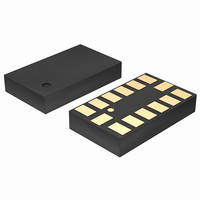
... Thresholds and timing of interrupt generators are programmable by the end user on the fly. The LIS302DLH is available in small thin plastic land grid array package (LGA) and it is guaranteed to operate over an extended temperature range from -40 °C to +85 °C. ...
Page 2
... I2C serial interface . . . . . . . . . . . . . . . . . . . . . . . . . . . . . . . . . . . . . . . . . . 17 5.1.1 5.2 SPI bus interface . . . . . . . . . . . . . . . . . . . . . . . . . . . . . . . . . . . . . . . . . . . 19 5.2.1 5.2.2 5.2.3 2/37 SPI - serial peripheral interface . . . . . . . . . . . . . . . . . . . . . . . . . . . . . . . 11 I2C - Inter IC control interface . . . . . . . . . . . . . . . . . . . . . . . . . . . . . . . . 12 Sensitivity . . . . . . . . . . . . . . . . . . . . . . . . . . . . . . . . . . . . . . . . . . . . . . . . 14 Zero-g level . . . . . . . . . . . . . . . . . . . . . . . . . . . . . . . . . . . . . . . . . . . . . . 14 Self-test . . . . . . . . . . . . . . . . . . . . . . . . . . . . . . . . . . . . . . . . . . . . . . . . . 14 Sleep to wake- I2C operation . . . . . . . . . . . . . . . . . . . . . . . . . . . . . . . . . . . . . . . . . . . . . 18 SPI read . . . . . . . . . . . . . . . . . . . . . . . . . . . . . . . . . . . . . . . . . . . . . . . . . 20 SPI write . . . . . . . . . . . . . . . . . . . . . . . . . . . . . . . . . . . . . . . . . . . . . . . . 21 SPI read in 3-wires mode . . . . . . . . . . . . . . . . . . . . . . . . . . . . . . . . . . . 22 Doc ID 15797 Rev 1 LIS302DLH ...
Page 3
... LIS302DLH 6 Register mapping . . . . . . . . . . . . . . . . . . . . . . . . . . . . . . . . . . . . . . . . . . 23 7 Register description . . . . . . . . . . . . . . . . . . . . . . . . . . . . . . . . . . . . . . . . 24 7.1 WHO_AM_I (0Fh 7.2 CTRL_REG1 (20h 7.3 CTRL_REG2 (21h 7.4 CTRL_REG3 [Interrupt CTRL register] (22h 7.5 CTRL_REG4 (23h 7.6 CTRL_REG5 (24h 7.7 HP_FILTER_RESET (25h 7.8 REFERENCE (26h 7.9 STATUS_REG (27h 7.10 OUT_X_L (28h), OUT_X_H (29h ...
Page 4
... INT1_CFG register . . . . . . . . . . . . . . . . . . . . . . . . . . . . . . . . . . . . . . . . . . . . . . . . . . . . . . . 27 Table 38. INT1_CFG description . . . . . . . . . . . . . . . . . . . . . . . . . . . . . . . . . . . . . . . . . . . . . . . . . . . . 27 Table 39. Interrupt 1 source configurations . . . . . . . . . . . . . . . . . . . . . . . . . . . . . . . . . . . . . . . . . . . . 28 Table 40. INT1_SRC register . . . . . . . . . . . . . . . . . . . . . . . . . . . . . . . . . . . . . . . . . . . . . . . . . . . . . . . 28 Table 41. INT1_SRC description . . . . . . . . . . . . . . . . . . . . . . . . . . . . . . . . . . . . . . . . . . . . . . . . . . . . 28 Table 42. INT1_THS register . . . . . . . . . . . . . . . . . . . . . . . . . . . . . . . . . . . . . . . . . . . . . . . . . . . . . . . 29 Table 43. INT1_THS description . . . . . . . . . . . . . . . . . . . . . . . . . . . . . . . . . . . . . . . . . . . . . . . . . . . . 29 Table 44. INT1_DURATION register . . . . . . . . . . . . . . . . . . . . . . . . . . . . . . . . . . . . . . . . . . . . . . . . . 29 Table 45. INT1_DURATION description . . . . . . . . . . . . . . . . . . . . . . . . . . . . . . . . . . . . . . . . . . . . . . . 29 Table 46. INT2_CFG register . . . . . . . . . . . . . . . . . . . . . . . . . . . . . . . . . . . . . . . . . . . . . . . . . . . . . . . 29 Table 48. Interrupt mode configuration . . . . . . . . . . . . . . . . . . . . . . . . . . . . . . . . . . . . . . . . . . . . . . . . 30 Table 47. INT2_CFG description . . . . . . . . . . . . . . . . . . . . . . . . . . . . . . . . . . . . . . . . . . . . . . . . . . . . 30 4/37 Doc ID 15797 Rev 1 LIS302DLH ...
Page 5
... LIS302DLH Table 49. INT2_SRC register . . . . . . . . . . . . . . . . . . . . . . . . . . . . . . . . . . . . . . . . . . . . . . . . . . . . . . . 30 Table 50. INT2_SRC description . . . . . . . . . . . . . . . . . . . . . . . . . . . . . . . . . . . . . . . . . . . . . . . . . . . . 31 Table 51. INT2_THS register . . . . . . . . . . . . . . . . . . . . . . . . . . . . . . . . . . . . . . . . . . . . . . . . . . . . . . . 31 Table 52. INT2_THS description . . . . . . . . . . . . . . . . . . . . . . . . . . . . . . . . . . . . . . . . . . . . . . . . . . . . 31 Table 53. INT2_DURATION register . . . . . . . . . . . . . . . . . . . . . . . . . . . . . . . . . . . . . . . . . . . . . . . . . 31 Table 54. INT2_DURATION description . . . . . . . . . . . . . . . . . . . . . . . . . . . . . . . . . . . . . . . . . . . . . . . 31 Table 55. Document revision history . . . . . . . . . . . . . . . . . . . . . . . . . . . . . . . . . . . . . . . . . . . . . . . . . 33 Doc ID 15797 Rev 1 List of tables 5/37 ...
Page 6
... Figure 1. Block diagram . . . . . . . . . . . . . . . . . . . . . . . . . . . . . . . . . . . . . . . . . . . . . . . . . . . . . . . . . . . . 6 Figure 2. Pin connection . . . . . . . . . . . . . . . . . . . . . . . . . . . . . . . . . . . . . . . . . . . . . . . . . . . . . . . . . . . 6 Figure 3. SPI slave timing diagram . . . . . . . . . . . . . . . . . . . . . . . . . . . . . . . . . . . . . . . . . . . . . . . . . . 10 Figure 4. I2C Slave timing diagram . . . . . . . . . . . . . . . . . . . . . . . . . . . . . . . . . . . . . . . . . . . . . . . . . . 11 Figure 5. LIS302DLH electrical connection . . . . . . . . . . . . . . . . . . . . . . . . . . . . . . . . . . . . . . . . . . . . 15 Figure 6. Read and write protocol . . . . . . . . . . . . . . . . . . . . . . . . . . . . . . . . . . . . . . . . . . . . . . . . . . . 19 Figure 7. SPI read protocol . . . . . . . . . . . . . . . . . . . . . . . . . . . . . . . . . . . . . . . . . . . . . . . . . . . . . . . . 19 Figure 8. Multiple bytes SPI read protocol (2 bytes example Figure 9. SPI write protocol . . . . . . . . . . . . . . . . . . . . . . . . . . . . . . . . . . . . . . . . . . . . . . . . . . . . . . . . 20 Figure 10 ...
Page 7
... LIS302DLH 1 Block diagram and pin description 1.1 Block diagram Figure 1. Block diagram a SELF TEST 1.2 Pin description Figure 2. Pin connection Y 6 TOP VIEW X+ CHARGE Y+ AMPLIFIER Z+ A/D MUX CONVERTER TRIMMING REFERENCE CIRCUITS Doc ID 15797 Rev 1 Block diagram and pin description CS SCL/SPC I2C ...
Page 8
... C less significant bit of the device address 2 SDA I C serial data (SDA) SDI SPI serial data input (SDI) SDO 3-wire interface serial data output (SDO) 2 SCL I C serial clock (SCL) SPC SPI serial port clock (SPC) Doc ID 15797 Rev 1 LIS302DLH Function 2 C mode; 0: SPI enabled) ...
Page 9
... LIS302DLH 2 Mechanical and electrical specifications 2.1 Mechanical characteristics Table 3. Mechanical characteristics @ Vdd = 2 °C unless otherwise noted Symbol Parameter FS Measurement range So Sensitivity Sensitivity change vs TCSo temperature g Typical zero- level offset TyOff (4),(5) accuracy g Zero- level change vs TCOff temperature An Acceleration noise density Self-test ...
Page 10
... DR bit set bit set bit set bit set bit set to 010 PM bit set to 011 PM bit set to 100 PM bit set to 101 PM bit set to 110 ODR = 100 Hz Doc ID 15797 Rev 1 LIS302DLH (1) (2) Min. Typ. Max. 2.16 2.5 3.6 1.71 Vdd+0.1 250 ...
Page 11
... LIS302DLH 2.3 Communication interface characteristics 2.3.1 SPI - serial peripheral interface Subject to general operating conditions for Vdd and Top. Table 5. SPI slave timing values Symbol tc(SPC) SPI clock cycle fc(SPC) SPI clock frequency tsu(CS) CS setup time th(CS) CS hold time tsu(SI) SDI input setup time ...
Page 12
... Max. 0 100 4.7 4.0 250 0.01 3.45 1000 300 4 4.7 4 4.7 ( h(SDA) su(SDA) r(SDA w(SCLH) r(SCL) f(SCL) Doc ID 15797 Rev 1 LIS302DLH ( fast mode Min. Max. 0 400 1.3 0.6 100 0.01 0.9 ( 0.1C 300 b ( 0.1C 300 b 0.6 0.6 0.6 1.3 REPEATED ...
Page 13
... LIS302DLH 2.4 Absolute maximum ratings Stresses above those listed as “absolute maximum ratings” may cause permanent damage to the device. This is a stress rating only and functional operation of the device under these conditions is not implied. Exposure to maximum rating conditions for extended periods may affect device reliability ...
Page 14
... The “sleep to wake-up” function, in conjunction with low-power mode, allows to further reduce the system power consumption and develop new smart applications. LIS302DLH may be set in a low-power operating mode, characterized by lower date rates refreshments. In this way the device, even if sleeping, keep on sensing acceleration and generating interrupt requests. When the “ ...
Page 15
... The acceleration data may be accessed through an I device particularly suitable for direct interfacing with a microcontroller. The LIS302DLH features a Data-Ready signal (RDY) which indicates when a new set of measured acceleration data is available thus simplifying data synchronization in the digital system that uses the device. ...
Page 16
... Application hints 4 Application hints Figure 5. LIS302DLH electrical connection Vdd 10uF 100nF GND The device core is supplied through Vdd line while the I/O pads are supplied through Vdd_IO line. Power supply decoupling capacitors (100 nF ceramic, 10 µF Aluminum) should be placed as near as possible to the pin 6 of the device (common design practice). ...
Page 17
... DAta line (SDA). The latter is a bidirectional line used for sending and receiving the data to/from the interface. Both the lines are connected to Vdd_IO through a pull-up resistor embedded inside the LIS302DLH. When the bus is free both the lines are high. 2 The I C interface is compliant with fast mode (400 kHz) I normal mode ...
Page 18
... If they match, the device considers itself addressed by the Master. The Slave ADdress (SAD) associated to the LIS302DLH is 001100xb. SDO/SA0 pad can be used to modify less significant bit of the device address. If SA0 pad is connected to voltage supply, LSb is ‘1’ (address 0011001b) else if SA0 pad is connected to ground, LSb value is ‘ ...
Page 19
... In the presented communication format MAK is Master acknowledge and NMAK is No Master Acknowledge. 5.2 SPI bus interface The LIS302DLH SPI is a bus slave. The SPI allows to write and read the registers of the device. The Serial Interface interacts with the outside world with 4 wires: CS, SPC, SDI and SDO. SAD + W ...
Page 20
... AD5 AD4 AD3 AD2 AD1 AD0 DO7 DO6 DO5 DO4 DO3 DO2 DO1 DO0 RW MS AD5 AD4 AD3 AD2 AD1 AD0 Doc ID 15797 Rev 1 DI7 DI6 DI5 DI4 DI3 DI2 DI1 DI0 DO7 DO6 DO5 DO4 DO3 DO2 DO1 DO0 LIS302DLH ...
Page 21
... LIS302DLH The SPI Read command is performed with 16 clock pulses. Multiple byte read command is performed adding blocks of 8 clock pulses at the previous one. bit 0: READ bit. The value is 1. bit 1: MS bit. When 0 do not increment address, when 1 increment address in multiple reading. ...
Page 22
... DI7 DI6 DI5 DI4 DI3 DI2 DI1 DI0 DI15 DI14 DI13 DI12 DI11 DI10 DI9 DI8 AD5 AD4 AD3 AD2 AD1 AD0 RW MS AD5 AD4 AD3 AD2 AD1 AD0 Doc ID 15797 Rev 1 DO7 DO6 DO5 DO4 DO3 DO2 DO1 DO0 LIS302DLH ...
Page 23
... LIS302DLH 6 Register mapping The table given below provides a listing of the 8 bit registers embedded in the device and the related addresses: Table 15. Register address map Name Reserved (do not modify) WHO_AM_I Reserved (do not modify) CTRL_REG1 CTRL_REG2 CTRL_REG3 CTRL_REG4 CTRL_REG5 HP_FILTER_RESET REFERENCE STATUS_REG OUT_X_L OUT_X_H ...
Page 24
... The registers address, made of 7 bits, is used to identify them and to write the data through serial interface. 7.1 WHO_AM_I (0Fh) Table 16. WHO_AM_I register 0 0 Device identification register. This register contains the device identifier that for LIS302DLH is set to 32h. 7.2 CTRL_REG1 (20h) Table 17. CTRL_REG1 register PM2 PM1 Table 18. CTRL_REG1 description Power mode selection ...
Page 25
... LIS302DLH data in the low-power modes are computed with low-pass filter cut-off frequency defined by DR1, DR0 bits. DR bits, in the normal-mode operation, select the data rate at which acceleration samples are produced. In low-power mode they define the output data resolution. the possible configuration for DR1 and DR0 bits. ...
Page 26
... Normal mode (reset reading HP_RESET_FILTER) ⎛ – ----------- - ⎝ t HPc --------------------- - f t ⋅ 6 HPc f [Hz] f [Hz Data rate = 100 0.5 1 0.25 0.5 0.125 0.25 Doc ID 15797 Rev 1 LIS302DLH High-pass filter mode t f ⎞ s ------ ⋅ ⎠ 2π f [Hz Data rate = 400 Hz Data rate = 1000 which is [Hz 2.5 ...
Page 27
... LIS302DLH 7.4 CTRL_REG3 [Interrupt CTRL register] (22h) Table 25. CTRL_REG3 register IHL PP_OD Table 26. CTRL_REG3 description Interrupt active high, low. Default value: 0 IHL (0: active high; 1:active low) Push-pull/Open drain selection on interrupt pad. Default value 0. PP_OD (0: push-pull; 1: open drain) Latch interrupt request on INT2_SRC register, with INT2_SRC register cleared by reading INT2_SRC itself ...
Page 28
... Setting TurnOn[1:0] bits to 11 the “sleep to wake” function is enabled. When an interrupt event occurs the device is turned to normal mode increasing the ODR to the value defined in 28/ TurnOn0 0 Sleep to wake function is disabled Turned on: The device is in low power mode (ODR is defined in 1 Doc ID 15797 Rev TurnOn1 Sleep to wake status CTRL_REG1) LIS302DLH TurnOn0 ...
Page 29
... LIS302DLH CTRL_REG1. Although the device is in normal mode, CTRL_REG1 content is not automatically changed to “normal mode” configuration. 7.7 HP_FILTER_RESET (25h) Dummy register. Reading at this address zeroes instantaneously the content of the internal high pass-filter. If the high pass filter is enabled all three axes are instantaneously set to 0g. ...
Page 30
... Enable interrupt generation on Z low event. Default value: 0 ZLIE (0: disable interrupt request; 1: enable interrupt request on measured accel. value lower than preset threshold) 30/37 ZHIE ZLIE Table 39) Table 39) Doc ID 15797 Rev 1 YHIE YLIE XHIE LIS302DLH XLIE ...
Page 31
... LIS302DLH Table 38. INT1_CFG description Enable interrupt generation on Y high event. Default value: 0 YHIE (0: disable interrupt request; 1: enable interrupt request on measured accel. value higher than preset threshold) Enable interrupt generation on Y low event. Default value: 0 YLIE (0: disable interrupt request; 1: enable interrupt request on measured accel. value lower than preset threshold) Enable interrupt generation on X high event ...
Page 32
... ODR chosen. 7.17 INT2_CFG (34h) Table 46. INT2_CFG register AOI 6D 32/37 THS5 THS4 Interrupt 1 threshold. Default value: 000 0000 D5 D4 Duration value. Default value: 000 0000 ZHIE ZLIE Doc ID 15797 Rev 1 THS3 THS2 THS1 YHIE YLIE XHIE LIS302DLH THS0 D0 XLIE ...
Page 33
... LIS302DLH Table 47. INT2_CFG description AND/OR combination of interrupt events. Default value: 0. AOI (See table below) 6 direction detection function enable. Default value (See table below) Enable interrupt generation on Z high event. Default value: 0 ZHIE (0: disable interrupt request; 1: enable interrupt request on measured accel. value higher than preset threshold) Enable interrupt generation on Z low event ...
Page 34
... bits set the minimum duration of the Interrupt 2 event to be recognized. Duration time steps and maximum values depend on the ODR chosen. 34/37 THS5 THS4 Interrupt 2 threshold. Default value: 000 0000 D5 D4 Duration value. Default value: 000 0000 Doc ID 15797 Rev 1 THS3 THS2 THS1 LIS302DLH THS0 D0 ...
Page 35
... LIS302DLH 8 Package information In order to meet environmental requirements, ST offers these devices in different grades of ® ECOPACK packages, depending on their level of environmental compliance. ECOPACK specifications, grade definitions and product status are available at: www.st.com. ECOPACK trademark. Figure 12. LGA-14: mechanical data and package dimensions MECHANICAL DATA ...
Page 36
... Revision history 9 Revision history Table 55. Document revision history Date 04-Jun-2009 36/37 Revision 1 Initial release Doc ID 15797 Rev 1 LIS302DLH Changes ...
Page 37
... LIS302DLH Information in this document is provided solely in connection with ST products. STMicroelectronics NV and its subsidiaries (“ST”) reserve the right to make changes, corrections, modifications or improvements, to this document, and the products and services described herein at any time, without notice. All ST products are sold pursuant to ST’s terms and conditions of sale. ...