LMH6503MA National Semiconductor, LMH6503MA Datasheet - Page 15

LMH6503MA
Manufacturer Part Number
LMH6503MA
Description
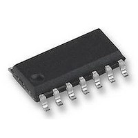
AMP, WIDEBAND, VARIABLE GAIN, 6503
Manufacturer
National Semiconductor
Datasheet
1.LMH6503MA.pdf
(20 pages)
Specifications of LMH6503MA
No. Of Amplifiers
1
Bandwidth
135MHz
Gain Accuracy
4.4dB
No. Of Channels
1
Supply Voltage Range
5V To 12V
Amplifier Case Style
SOIC
No. Of Pins
14
Operating Temperature Range
-40°C To +85°C
Lead Free Status / RoHS Status
Lead free / RoHS Compliant
Available stocks
Company
Part Number
Manufacturer
Quantity
Price
Part Number:
LMH6503MA
Manufacturer:
NS/国半
Quantity:
20 000
Company:
Part Number:
LMH6503MAX/NOPB
Manufacturer:
NS
Quantity:
7 985
Application Information
the minimum possible values that meet the input voltage and
maximum gain constraints. Scaling the resistor values will
decrease bandwidth and improve stability.
Figure 2 illustrates the resulting LMH6503 bandwidths as a
function of the maximum ( y axis) and minimum (related to x
axis) input voltages when V
ADJUSTING OFFSETS
Treating the offsets introduced by the input and output
stages of the LMH6503 is accomplished with a two step
process. The offset voltage of the output stage is treated by
first applying −1.1V on V
input stage and multiplier core from the output stage. As
illustrated in Figure 3, the trim pot located at R14 on the
LMH6503 Evaluation Board (CLC730033) should then be
adjusted in order to null the offset voltage seen at the
LMH6503’s output (pin 10).
FIGURE 3. Nulling the Output Offset Voltage
FIGURE 2. Bandwidth vs. V
G
OUT
, which effectively isolates the
is held constant at 1V
INMAX
and A
(Continued)
20073902
VMAX
20073954
PP
.
(5)
15
Once this is accomplished, the offset errors introduced by
the input stage and multiplier core can then be treated. The
second step requires the absence of an input signal and
matched source impedances on the two input pins in order to
cancel the bias current errors. This done, then +1.1V should
be applied to V
order to null the offset voltage seen at the LMH6503’s output.
If a more limited gain range is anticipated, the above adjust-
ments should be made at these operating points. These
steps will minimize the output offset voltage. However, since
the offset term itself varies with the gain setting, the correc-
tion is not perfect and some residual output offset will re-
main.
GAIN ACCURACY
Defined as the ratio of measured gain (V/V), at a certain V
to the best fit line drawn through the typical gain (V/V)
distribution for −1V
(See Figure 4). The best fit gain (A
For a V
the worst case accuracy over the entire range. The "Typical"
value would be the worst case ratio between the "Typical
Gain" and the best fit line. The "Max" value would be the
worst case between the max/min gain limit and the best fit
line.
GAIN MATCHING
Defined as the limit on gain variation at a certain V
pressed in dB) (See Figure 4). Specified as "Max" only (no
"Typical"). For a V
worst case matching over the entire range. The "Max" value
would be the worst case ratio between the max/min gain limit
and the typical gain.
FIGURE 4. Gain Accuracy and Gain Matching
For: −1V ≤ V
G
range, the value specified in the tables represents
G
A
and the trim pot located at R
G
V
Parameters Defined
range, the value specified represents the
G
(V/V) = 4.87V
<
≤ + 1V, R
V
G
<
1V (results expressed in dB)
F
= 1kΩ, R
G
V
+ 4.61
) is given by:
G
= 174Ω
10
www.national.com
adjusted in
20073955
G
(ex-
(6)
G
,


