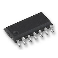
LMH6503MA National Semiconductor, LMH6503MA Datasheet - Page 14

LMH6503MA
Manufacturer Part Number
LMH6503MA
Description
AMP, WIDEBAND, VARIABLE GAIN, 6503
Manufacturer
National Semiconductor
Datasheet
1.LMH6503MA.pdf
(20 pages)
Specifications of LMH6503MA
No. Of Amplifiers
1
Bandwidth
135MHz
Gain Accuracy
4.4dB
No. Of Channels
1
Supply Voltage Range
5V To 12V
Amplifier Case Style
SOIC
No. Of Pins
14
Operating Temperature Range
-40°C To +85°C
Lead Free Status / RoHS Status
Lead free / RoHS Compliant
Available stocks
Company
Part Number
Manufacturer
Quantity
Price
Part Number:
LMH6503MA
Manufacturer:
NS/国半
Quantity:
20 000
Company:
Part Number:
LMH6503MAX/NOPB
Manufacturer:
NS
Quantity:
7 985
www.national.com
Typical Performance Charateristics
= 0V, R
output: (Continued)
Application Information
THEORY OF OPERATION
The LMH6503 is a linear wideband variable-gain amplifier as
illustrated in Figure 1. A voltage input signal may be applied
differentially between the two inputs (+V
endedly by grounding one of the two unused inputs. The
LMH6503 input buffers convert the input voltage to a current
(I
= (+V
(R
a current gain of K (1.72 nominal). The voltage controlled
two-quadrant multiplier attenuates this current which is then
converted to a voltage via the output amplifier. This output
amplifier is a current feedback op amp configured as a
Transimpedance amplifier. Its Transimpedance gain is the
feedback resistor (R
control are all voltages. The output voltage can easily be
calculated as shown in Equation 1:
Where K = 1.72 (Nominal)
since:
The gain of the LMH6503 is therefore a function of three
external variables: R
2:
The gain control voltage (V
maximum as expressed in Equation 3:
<
RG
G
V
). This current (I
G
) that is a function of the differential input voltage (V
IN
<
) - (−V
F
+1V. At V
= 1kΩ, R
IN
)) and the value of the gain setting resistor
G
G
RG
= +1V, the gain of the LMH6503 is at its
G
= 174Ω, both inputs terminated in 50Ω, R
F
, R
). The input signal, output, and gain
) is then mirrored to a gain stage with
F
, and V
G
) has an ideal input range of −1V
G
as expressed in Equation
IN
, −V
IN
), or single-
INPUT
V
G
(1)
(2)
Feedthrough
Unless otherwise specified: V
14
L
= 100Ω, Typical values, results referred to device
Notice also that Equation 3 holds for both differential and
single ended operation.
CHOOSING R
R
mum peak
input voltage (V
the maximum allowable current through R
2.3mA. Once A
and desired output voltages, R
Equation 5. These values of R
G
is calculated from Equation 4. V
FIGURE 1. LMH6503 Functional Block Diagram
F
20073982
VMAX
pk
AND R
) determined by the application. I
is determined from the minimum input
S
G
=
±
5V, 25˚C, V
F
F
and R
is then determined using
INPUTMAX
G
G
are
= V
G
and is typically
G_MAX
is the maxi-
RGMAX
, V
20073951
CM
(3)
(4)
is


