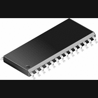
CS8415A-CS Cirrus Logic Inc, CS8415A-CS Datasheet - Page 13

CS8415A-CS
Manufacturer Part Number
CS8415A-CS
Description
IC, DIGITAL AUDIO RECEIVER, SOIC-28
Manufacturer
Cirrus Logic Inc
Specifications of CS8415A-CS
Audio Control Type
Digital
Control Interface
I2C, Serial
Control / Process Application
AV & DVD Receivers, CD-R, Digital Mixing Consoles
Supply Voltage Range
2.85V To 5.5V
Lead Free Status / RoHS Status
Contains lead / RoHS non-compliant
Available stocks
Company
Part Number
Manufacturer
Quantity
Price
Part Number:
CS8415A-CS
Manufacturer:
CIRRUS
Quantity:
20 000
Company:
Part Number:
CS8415A-CSR
Manufacturer:
CirrusLogic
Quantity:
569
Company:
Part Number:
CS8415A-CSZ
Manufacturer:
CIRRUS
Quantity:
108
Part Number:
CS8415A-CSZ
Manufacturer:
CRYSTAL
Quantity:
20 000
5. AES3 RECEIVER
The CS8415A includes an AES3 digital audio re-
ceiver. A comprehensive buffering scheme pro-
vides read access to the channel status and user
data. This buffering scheme is described in Appen-
dix B.
The AES3 receiver accepts and decodes audio and
digital data according to the AES3, IEC60958
(S/PDIF), and EIAJ CP-1201 interface standards.
The receiver consists of a differential input stage,
driven through pins RXP0 and RXN0, a PLL based
clock recovery circuit, and a decoder which sepa-
rates the audio data from the channel status and
user data.
External components are used to terminate and iso-
late the incoming data cables from the CS8415A.
These components are detailed in Appendix A.
5.1
The CS8415A employs a 7:1 S/PDIF Input Multi-
plexer to accommodate up to seven channels of in-
put digital audio data. Digital audio data is single-
ended and input through the RXP0-6 pins. When
any portion of the multiplexer is implemented, un-
used RXP pins should be tied to ground, and RXN0
must be ac-coupled to ground. The multiplexer se-
lect line control is accessed through bits MUX2:0
in the Control 2 register. The multiplexer defaults
to RXP0. Therefore, the default configuration is for
a differential signal to be input through RXP0 &
RXN0. Please see Appendix A for recommended
input circuits.
5.2
An on-chip Phase Locked Loop (PLL) is used to re-
cover the clock from the incoming data stream.
There are some applications where low jitter in the
recovered clock, presented on the RMCK pin, is
important. For this reason, the PLL has been de-
signed to have good jitter attenuation characteris-
tics, shown in Figures 7 and 8. In addition, the PLL
DS470PP3
7:1 S/PDIF Input Multiplexer
PLL, Jitter Attenuation, and
Varispeed
has been designed to only use the preambles of the
AES3 stream to provide lock update information to
the PLL. This results in the PLL being immune to
data dependent jitter affects because the AES3 pre-
ambles do not vary with the data.
The PLL has the ability to lock onto a wide range
of input sample rates with no external component
changes. If the sample rate of the input subsequent-
ly changes, for example in a varispeed application,
the PLL will only track up to ±12.5% from the
nominal center sample rate. The nominal center
sample rate is the sample rate that the PLL first
locks onto upon application of an AES3 data
stream or after enabling the CS8415A clocks by
setting the RUN control bit. If the 12.5% sample
rate limit is exceeded, the PLL will return to its
wide lock range mode and re-acquire a new nomi-
nal center sample rate.
5.2.1
A special clock switching mode is available that al-
lows the clock that is input through the OMCK pin
to be output through the RMCK pin. This feature is
controlled by the SWCLK bit in register 1 of the
control registers. When the PLL loses lock, the fre-
quency of the VCO drops to 300 kHz. The clock
switching mode allows the clock input through
OMCK to be used as a clock in the system without
any disruption when the PLL loses lock, for exam-
ple, when the input is removed from the receiver.
When SWCLK is enabled and this mode is imple-
mented, RMCK is an output and is not bi-direction-
al. This clock switching is done glitch free. Please
note that internal circuitry associated with RMCK
is not driven by OMCK. This means that OSCLK
and OLRCK continue to be derived from the PLL
and are not usable in this mode.
5.2.2
The PLL behavior is affected by the external filter
component values. Figure 5 shows the recom-
mended configuration of the two capacitors and
OMCK System Clock Mode
PLL External Components
CS8415A
13


