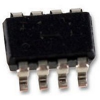
HT1381-8SOPLF HOLTEK, HT1381-8SOPLF Datasheet - Page 6

HT1381-8SOPLF
Manufacturer Part Number
HT1381-8SOPLF
Description
IC, TIMEKEEPER, SERIAL, SMD, SOP8
Manufacturer
HOLTEK
Datasheet
1.HT1381-8SOPLF.pdf
(10 pages)
Specifications of HT1381-8SOPLF
Clock Format
HH
Clock Ic Type
Timekeeper
Supply Voltage Range
2V To 5.5V
Digital Ic Case Style
SOP
No. Of Pins
8
Operating Temperature Range
0°C To +70°C
Date Format
DD
Lead Free Status / RoHS Status
Lead free / RoHS Compliant
Write protect register
This register is used to prevent a write opera-
tion to any other register. Data can be written
into the designated register only if the Write
Protect signal (WP) is set to logic 0. The Write
Protect Register should be set first before re-
starting the system or before writing the new
data to the system, and it should set as logic 1 in
the read cycle. The Write Protect bit cannot be
written to in the burst mode.
Clock Halt bit
D7 of the Seconds Register is defined as the
Clock Halt Flag (CH).
When this bit is set to logic 1, the clock oscilla-
tor is stopped and the chip goes into a
low-power standby mode. When this bit is writ-
ten to logic 0, the clock will start.
12-hour/24-hour mode
The D7 of the hour register is defined as the
12-hour or 24-hour mode select bit.
When this bit is in high level, the 12-hour mode
is selected otherwise it¢s the 24-hour mode.
AM-PM mode
These are two functions for the D5 of the hour
register determined by the value D7 of the same
register.
One is used in AM/PM selection on the 12-hour
mode. When D5 is logic 1, it is PM, otherwise
it¢s AM. The other is used to set the second
10-hour bit (20~23 hours) on the 24-hour mode.
Reset and Serial Clock control
The REST pin is used to allow access data to the
shift register like a toggle switch. When the
REST pin is taken high, the built-in control
logic is turned on and the address/command se-
quence can access the corresponding shift regis-
ter. The REST pin is also used to terminate
either single-byte or burst mode data format.
6
The input signal of SCLK is a sequence of a fall-
ing edge followed by a rising edge and it is used
to synchronize the register data whether read
or write. For data input, the data must be read
after the rising edge of SCLK. The data on the
I/O pin becomes output mode after the falling
edge of the SCLK. All data transfer terminates
if the REST pin is low and the I/O pin goes to a
high impedance state. The data transfer is il-
lustrated on the next page.
Data in and Data out
In writing a data byte with HT1380/HT1381,
the read/write should first set as R/W=0 in the
Command Byte and follow with the correspond-
ing data register on the rising edge of the next
eight SCLK cycles. Additional SCLK cycles are
ignored. Data inputs are entered starting with
bit 0.
I n re a ding a da ta o n the registe r of
HT1380/HT1381, R/W=1 should first be en-
tered as input. The data bit outputs on the fall-
ing edge of the next eight SCLK cycles. Note
that the first data bit to be transmitted on the
first falling edge after the last bit of the read
command byte is written. Additional SCLK cy-
cles re-transmits the data bytes as long as
REST remains at high level. Data outputs are
read starting with bit 0.
Crystal selection
A 32768Hz crystal can be directly connected to
the HT1380/HT1381 via pin 2 and pin 3 (X1,
X2). In order to obtain the correct frequency,
two additional load capacities (C1, C2) are
needed. The value of the capacity depends on
how accurate the crystal is. We suggest that
you can follow the table on the next page.
HT1380/HT1381
September 18, 2000


