UBA2028T/N1 NXP Semiconductors, UBA2028T/N1 Datasheet - Page 8

UBA2028T/N1
Manufacturer Part Number
UBA2028T/N1
Description
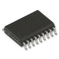
CFL DRIVER, 600V, DIMMABLE, 20SOIC
Manufacturer
NXP Semiconductors
Datasheet
1.UBA2028TN1518.pdf
(23 pages)
Specifications of UBA2028T/N1
Module Configuration
Half Bridge
Supply Current
170µA
Meter Display Type
Fluorescent Lamp
Supply Voltage Range
8.6V To 9.6V, 12.4V To 13.6V
Driver Case Style
SOIC
No. Of Pins
20
Operating
RoHS Compliant
Available stocks
Company
Part Number
Manufacturer
Quantity
Price
Part Number:
UBA2028T/N1
Manufacturer:
NXP/恩智浦
Quantity:
20 000
NXP Semiconductors
UBA2028
Product data sheet
8.10 Capacitive mode protection
8.12 Design equations
8.11 Charge coupling
8.9 Power-down mode
lamp. If during restart the lamp still fails, the voltage remains high until the end of the
ignition time. At the end of the ignition time the circuit stops oscillating and the circuit will
enter the Power-down mode.
The Power-down mode will be entered if, at the end of the ignition time, the voltage at pin
LVS is above V
TR1 and TR2 will be non-conductive. The V
released from the Power-down mode by lowering the low voltage supply below V
The signal across R15 see
switching behavior of the half-bridge. If, after the preheat state, the voltage across the
ACM resistor (R15 or R6) does not exceed the V
time, the Capacitive Mode Detection circuit (CMD) assumes that the circuit is in the
capacitive mode of operation. As a consequence the frequency will directly be increased
to f
been discharged to zero.
Due to parasitic capacitive coupling to the high voltage circuitry all pins are burdened with
a repetitive charge injection. Given the typical application the pins IREF and CF are
sensitive to this charge injection. For charge coupling of approximately 8 pC, a safe
functional operation of the IC is guaranteed, independent of the current level.
Charge coupling at current levels below 50 μA will not interfere with the accuracy of the
V
Charge coupling at current levels below 20 μA will not interfere with the accuracy of any
parameter.
The following design equations are used to calculate the desired preheat time, the
maximum ignition time, and the minimum and the maximum switching frequency.
Start of ignition is defined as the moment at which the measured lamp voltage crosses the
V
t
t
f
f
ph
ign
min
CS
lamp(fail)
max
max
, V
=
=
=
=
. The frequency behavior is de coupled from the voltage at pin CSW until C
1.8
i(PCS)
0.26
40.5
2.5
level; see
×
×
------------------------- -
330
×
and V
×
------------------------- -
330
f
10
min
C
lamp(fail)
×
All information provided in this document is subject to legal disclaimers.
CT
C
3
×
10
×
CT
i(ACM)
10
Section
100
--------------------------- -
9 –
9 –
×
. In the Power-down mode the oscillator will be stopped and both
C
×
Rev. 02 — 19 July 2010
×
------------------- -
33
levels.
CF
R
10
------------------- -
33
IREF
×
R
Figure 8
8.8.
–
IREF
10
×
12
600 V dimmable power IC for compact fluorescent lamps
10
3
×
3
33
------------------- -
R
IREF
×
(R6 in
10
3
Figure
DD
supply is internally clamped. The circuit is
det(capm)
9) also gives information about the
level during the non-overlap
UBA2028
© NXP B.V. 2010. All rights reserved.
DD(rst)
CSW
8 of 23
has
.
(1)
(2)
(3)
(4)


