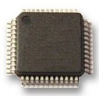
SC16C650BIB48 NXP Semiconductors, SC16C650BIB48 Datasheet - Page 26

SC16C650BIB48
Manufacturer Part Number
SC16C650BIB48
Description
UART, 32BYTE FIFO, 16C650, LQFP48
Manufacturer
NXP Semiconductors
Datasheet
1.SC16C650BIB48151.pdf
(48 pages)
Specifications of SC16C650BIB48
No. Of Channels
1
Data Rate
3Mbps
Supply Voltage Range
2.25V To 5.5V
Operating Temperature Range
-40°C To +85°C
Digital Ic Case Style
LQFP
No. Of Pins
48
Svhc
No SVHC (18-Jun-2010)
Operating
RoHS Compliant
Uart Features
Automatic Software/Hardware Flow Control, Programmable Xon/Xoff Characters
Rohs Compliant
Yes
Available stocks
Company
Part Number
Manufacturer
Quantity
Price
Company:
Part Number:
SC16C650BIB48,151
Manufacturer:
NXP Semiconductors
Quantity:
10 000
Company:
Part Number:
SC16C650BIB48151
Manufacturer:
NXP Semiconductors
Quantity:
135
NXP Semiconductors
SC16C650B_4
Product data sheet
7.8 Modem Status Register (MSR)
This register provides the current state of the control interface signals from the modem, or
other peripheral device to which the SC16C650B is connected. Four bits of this register
are used to indicate the changed information. These bits are set to a logic 1 whenever a
control input from the modem changes state. These bits are set to a logic 0 whenever the
CPU reads this register.
Table 21.
[1]
Bit
7
6
5
4
3
2
1
0
Whenever any MSR bit 3:0 is set to logic 1, a Modem Status Interrupt will be generated.
Symbol
MSR[7]
MSR[6]
MSR[5]
MSR[4]
MSR[3]
MSR[2]
MSR[1]
MSR[0]
Modem Status Register bits description
Description
Data Carrier Detect. DCD (active HIGH, logic 1). Normally this bit is the
complement of the DCD input. In the loopback mode this bit is equivalent to the
OUT2 bit in the MCR register.
Ring Indicator. RI (active HIGH, logic 1). Normally this bit is the complement of
the RI input. In the loopback mode this bit is equivalent to the OUT1 bit in the
MCR register.
Data Set Ready. DSR (active HIGH, logic 1). Normally this bit is the
complement of the DSR input. In loopback mode this bit is equivalent to the
DTR bit in the MCR register.
Clear To Send. CTS. CTS functions as hardware flow control signal input if it is
enabled via EFR[7]. Flow control (when enabled) allows starting and stopping
the transmissions based on the external modem CTS signal. A logic 1 at the
CTS pin will stop SC16C650B transmissions as soon as current character has
finished transmission. Normally MSR[4] is the complement of the CTS input.
However, in the loopback mode, this bit is equivalent to the RTS bit in the MCR
register.
DCD
RI
DSR
CTS
logic 0 = no DCD change (normal default condition)
logic 1 = the DCD input to the SC16C650B has changed state since the last
time it was read. A modem Status Interrupt will be generated.
logic 0 = no RI change (normal default condition)
logic 1 = the RI input to the SC16C650B has changed from a logic 0 to a
logic 1. A modem Status Interrupt will be generated.
logic 0 = no DSR change (normal default condition)
logic 1 = the DSR input to the SC16C650B has changed state since the last
time it was read. A modem Status Interrupt will be generated.
logic 0 = no CTS change (normal default condition)
logic 1 = the CTS input to the SC16C650B has changed state since the last
time it was read. A modem Status Interrupt will be generated.
Rev. 04 — 14 September 2009
[1]
[1]
[1]
[1]
UART with 32-byte FIFOs and IrDA encoder/decoder
SC16C650B
© NXP B.V. 2009. All rights reserved.
26 of 48


