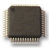
SC16C752BIB48 NXP Semiconductors, SC16C752BIB48 Datasheet - Page 22

SC16C752BIB48
Manufacturer Part Number
SC16C752BIB48
Description
IC, UART, DUAL, 64BYTE FIFO, 16C752
Manufacturer
NXP Semiconductors
Datasheet
1.SC16C752BIBS128.pdf
(47 pages)
Specifications of SC16C752BIB48
No. Of Channels
2
Data Rate
5Mbps
Supply Voltage Range
2.25V To 5.5V
Operating Temperature Range
-40°C To +85°C
Digital Ic Case Style
LQFP
No. Of Pins
48
Svhc
No SVHC (18-Jun-2010)
Uart Features
DMA Signalling Capability, Software Selectable Baud Rate Generator
Rohs Compliant
Yes
Lead Free Status / RoHS Status
Lead free / RoHS Compliant
Available stocks
Company
Part Number
Manufacturer
Quantity
Price
Company:
Part Number:
SC16C752BIB48
Manufacturer:
NXP Semiconductors
Quantity:
1 940
Company:
Part Number:
SC16C752BIB48
Manufacturer:
TI
Quantity:
430
Part Number:
SC16C752BIB48
Manufacturer:
NXP/恩智浦
Quantity:
20 000
Company:
Part Number:
SC16C752BIB48,128
Manufacturer:
NXP Semiconductors
Quantity:
10 000
Company:
Part Number:
SC16C752BIB48,151
Manufacturer:
NXP Semiconductors
Quantity:
10 000
Company:
Part Number:
SC16C752BIB48,157
Manufacturer:
NXP Semiconductors
Quantity:
10 000
NXP Semiconductors
SC16C752B
Product data sheet
7.3 FIFO Control Register (FCR)
This is a write-only register that is used for enabling the FIFOs, clearing the FIFOs, setting
transmitter and receiver trigger levels, and selecting the type of DMA signalling.
shows FIFO control register bit settings.
Table 11.
Bit
7:6
5:4
3
2
1
0
Symbol
FCR[7] (MSB),
FCR[6] (LSB)
FCR[5] (MSB),
FCR[4] (LSB)
FCR[3]
FCR[2]
FCR[1]
FCR[0]
FIFO Control Register bits description
All information provided in this document is subject to legal disclaimers.
5 V, 2.2 V and 2.5 V dual UART, 5 Mbit/s (max.), with 64-byte FIFOs
DMA mode select.
Rev. 6 — 30 November 2010
Description
RX trigger. Sets the trigger level for the receive FIFO.
TX trigger. Sets the trigger level for the transmit FIFO.
FCR[5:4] can only be modified and enabled when EFR[4] is set. This is
because the transmit trigger level is regarded as an enhanced function.
Reset transmit FIFO.
Reset receive FIFO.
FIFO enable.
00 - 8 characters
01 - 16 characters
10 - 56 characters
11 - 60 characters
00 - 8 spaces
01 - 16 spaces
10 - 32 spaces
11 - 56 spaces
logic 0 = set DMA mode ‘0’
logic 1 = set DMA mode ‘1’
logic 0 = no FIFO transmit reset (normal default condition)
logic 1 = Clears the contents of the transmit FIFO and resets the FIFO
counter logic (the transmit shift register is not cleared or altered). This bit
will return to a logic 0 after clearing the FIFO.
logic 0 = no FIFO receive reset (normal default condition)
logic 1 = Clears the contents of the receive FIFO and resets the FIFO
counter logic (the receive shift register is not cleared or altered). This bit
will return to a logic 0 after clearing the FIFO.
logic 0 = disable the transmit and receive FIFO (normal default
condition)
logic 1 = enable the transmit and receive FIFO.
SC16C752B
© NXP B.V. 2010. All rights reserved.
Table 11
22 of 47


