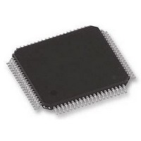
SC16C754BIB80 NXP Semiconductors, SC16C754BIB80 Datasheet - Page 27

SC16C754BIB80
Manufacturer Part Number
SC16C754BIB80
Description
IC, UART, QUAD, 64BYTE FIFO, 16C754
Manufacturer
NXP Semiconductors
Datasheet
1.SC16C754BIA68.pdf
(51 pages)
Specifications of SC16C754BIB80
No. Of Channels
4
Data Rate
5Mbps
Supply Voltage Range
2.25V To 5.5V
Operating Temperature Range
-40°C To +85°C
Digital Ic Case Style
LQFP
No. Of Pins
80
Svhc
No SVHC (18-Jun-2010)
Uart Features
DMA Signalling Capability, Software Selectable Baud Rate Generator
Rohs Compliant
Yes
Lead Free Status / RoHS Status
Lead free / RoHS Compliant
Available stocks
Company
Part Number
Manufacturer
Quantity
Price
Company:
Part Number:
SC16C754BIB80
Manufacturer:
NXP Semiconductors
Quantity:
1 780
Part Number:
SC16C754BIB80
Manufacturer:
NXP/恩智浦
Quantity:
20 000
Company:
Part Number:
SC16C754BIB80,528
Manufacturer:
NXP Semiconductors
Quantity:
10 000
Company:
Part Number:
SC16C754BIB80,551
Manufacturer:
NXP Semiconductors
Quantity:
10 000
Company:
Part Number:
SC16C754BIB80,557
Manufacturer:
NXP Semiconductors
Quantity:
10 000
NXP Semiconductors
SC16C754B_4
Product data sheet
7.6 Modem Control Register (MCR)
The MCR controls the interface with the modem, data set, or peripheral device that is
emulating the modem.
Table 14.
[1]
Bit
7
6
5
4
3
2
1
0
MCR[7:5] can only be modified when EFR[4] is set, that is, EFR[4] is a write enable.
Symbol
MCR[7]
MCR[6]
MCR[5]
MCR[4]
MCR[3]
MCR[2]
MCR[1]
MCR[0]
Modem control register bits description
[1]
[1]
[1]
5 V, 3.3 V and 2.5 V quad UART, 5 Mbit/s (max.) with 64-byte FIFOs
Rev. 04 — 6 October 2008
Description
Clock select.
TCR and TLR enable.
Xon Any.
Enable loopback.
IRQ enable OP.
FIFO Ready enable.
RTS
DTR
Table 14
logic 0 = divide-by-1 clock input
logic 1 = divide-by-4 clock input
logic 0 = no action
logic 1 = enable access to the TCR and TLR registers
logic 0 = disable Xon Any function
logic 1 = enable Xon Any function
logic 0 = normal operating mode
logic 1 = enable local loopback mode (internal). In this mode the
MCR[3:0] signals are looped back into MSR[7:4] and the TX output is
looped back to the RX input internally.
logic 0 = forces INTA to INTD outputs to the 3-state mode and OP
output to HIGH state
logic 1 = forces the INTA to INTD outputs to the active state and OP
output to LOW state. In loopback mode, controls MSR[7].
logic 0 = disable the FIFO Rdy register
logic 1 = enable the FIFO Rdy register. In loopback mode, controls
MSR[6].
logic 0 = force RTS output to inactive (HIGH)
logic 1 = force RTS output to active (LOW). In loopback mode, controls
MSR[4]. If auto-RTS is enabled, the RTS output is controlled by
hardware flow control.
logic 0 = force DTR output to inactive (HIGH)
logic 1 = force DTR output to active (LOW). In loopback mode, controls
MSR[5].
shows modem control register bit settings.
SC16C754B
© NXP B.V. 2008. All rights reserved.
27 of 51


