S25FL128P0XMFI001 Spansion Inc., S25FL128P0XMFI001 Datasheet - Page 30
S25FL128P0XMFI001
Manufacturer Part Number
S25FL128P0XMFI001
Description
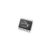
IC, FLASH, 128MBIT, 104MHZ, SOIC-16
Manufacturer
Spansion Inc.
Datasheet
1.S25FL128P0XMFI001.pdf
(49 pages)
Specifications of S25FL128P0XMFI001
Memory Type
Flash
Memory Size
128Mbit
Ic Interface Type
Serial, SPI
Clock Frequency
104MHz
Supply Voltage Range
2.7 To 3.6 V
Memory Case Style
SOIC
No. Of Pins
16
Data Bus Width
1 bit
Architecture
Uniform
Interface Type
SPI Serial
Supply Voltage (max)
3.6 V
Supply Voltage (min)
2.7 V
Maximum Operating Current
26 mA
Mounting Style
SMD/SMT
Operating Temperature
+ 85 C
Package / Case
SO-16
Cell Type
NOR
Density
128Mb
Boot Type
Not Required
Address Bus
1b
Operating Supply Voltage (typ)
3/3.3V
Package Type
SOIC W
Program/erase Volt (typ)
2.7 to 3.6V
Operating Temp Range
-40C to 85C
Operating Temperature Classification
Industrial
Operating Supply Voltage (min)
2.7V
Operating Supply Voltage (max)
3.6V
Word Size
1b
Number Of Words
128Mword
Supply Current
22mA
Mounting
Surface Mount
Pin Count
16
Rohs Compliant
Yes
Lead Free Status / RoHS Status
Lead free / RoHS Compliant
Lead Free Status / RoHS Status
Lead free / RoHS Compliant, Lead free / RoHS Compliant
Available stocks
Company
Part Number
Manufacturer
Quantity
Price
Company:

Part Number:
S25FL128P0XMFI001
Manufacturer:
HARRIS
Quantity:
2 300
Part Number:
S25FL128P0XMFI001
Manufacturer:
SPANSIO
Quantity:
20 000


Note
As defined by the values in the Block Protect (BP2, BP1, BP0) bits of the Status Register, as shown in
11.9
30
WP#/ACC
11.9.1
Signal
1
1
0
0
Page Program (PP: 02h)
Serial Mode
SRWD Bit
Table 11.5
HPM either by setting the SRWD bit after driving WP#/ACC low, or by driving WP#/ACC low after setting the
SRWD bit. However, the device disables HPM only when WP#/ACC is driven high.
Note that HPM only protects against changes to the status register. Since BP2:BP0 (or BP3:BP0) cannot be
changed in HPM, the size of the protected area of the memory array cannot be changed. Note that HPM
provides no protection to the memory array area outside that specified by Block Protect bits (Software
Protected Mode, or SPM).
If WP#/ACC is permanently tied high, HPM can never be activated, and only the SPM (Block Protect bits of
the Status Register) can be used.
The Page Program (PP) command changes specified bytes in the memory array (from 1 to 0 only). A WREN
command is required prior to writing the PP command.
The host system must drive CS# low, and then write the PP command, three address bytes, and at least one
data byte on SI. CS# must be driven low for the entire duration of the PP sequence. The command sequence
is shown in
The device programs only the last 256 data bytes sent to the device. If the number of data bytes exceeds this
limit, the bytes sent before the last 256 bytes are discarded, and the device begins programming the last 256
bytes sent at the starting address of the specified page. This may result in data being programmed into
different addresses within the same page than expected. If fewer than 256 data bytes are sent to device, they
are correctly programmed at the requested addresses.
The host system must drive CS# high after the device has latched the 8th bit of the data byte, otherwise the
device does not execute the PP command. The PP operation begins as soon as CS# is driven high. The
device internally controls the timing of the operation, which requires a period of t
be read to check the value of the Write In Progress (WIP) bit while the PP operation is in progress. The WIP
bit is 1 during the PP operation, and is 0 when the operation is completed. The device internally resets the
Write Enable Latch to 0 before the operation completes (the exact timing is not specified).
The device does not execute a Page Program (PP) command that specifies a page that is protected by the
Block Protect bits (see
1
0
0
1
Software
Protected
(SPM)
Hardware
Protected
(HPM)
shows that neither WP#/ACC or SRWD bit by themselves can enable HPM. The device can enter
Figure 11.14
Mode
Status Register is writable (if the WREN
command has set the WEL bit). The values in
the SRWD, BP2, BP1 and BP0 (or BP3, BP2,
BP1 and BP0) bits can be changed.
Status Register is Hardware write protected.
The values in the SRWD, BP2, BP1 and BP0
(or BP3, BP2, BP1 and BP0) bits cannot be
changed.
Table 7.1 on page
Write Protection of the Status Register
and
Table
Table 11.5 Protection Modes
11.6.
S25FL128P
13).
D a t a
S h e e t
Table 7.1 on page
Protected against program
Protected against program
and erase commands
and erase commands
Protected Area
(See Note)
S25FL128P_00_08 September 8, 2009
13.
PP
. The Status Register may
Program and Sector Erase
Program and Sector Erase
Ready to accept Page
Ready to accept Page
Unprotected Area
(See Note)
commands
commands
Related parts for S25FL128P0XMFI001
Image
Part Number
Description
Manufacturer
Datasheet
Request
R

Part Number:
Description:
128 Megabit Cmos 3.0 Volt Flash Memory With 104 Mhz Spi Serial Peripheral Interface Bus
Manufacturer:
Meet Spansion Inc.
Datasheet:

Part Number:
Description:
Flash 3V 32Mb Float Gate two address 90s
Manufacturer:
Spansion Inc.
Datasheet:
Part Number:
Description:
Flash 3V 64Mb Float Gate two address 90s
Manufacturer:
Spansion Inc.
Datasheet:

Part Number:
Description:
Flash 3V 64Mb Float Gate standard config 90s
Manufacturer:
Spansion Inc.
Datasheet:

Part Number:
Description:
Flash 3V 1 Gb Mirrorbit highest address120ns
Manufacturer:
Spansion Inc.
Datasheet:

Part Number:
Description:
Flash 3V 256Mb Mirrorbit highest address110ns
Manufacturer:
Spansion Inc.
Datasheet:
Part Number:
Description:
Flash 3V 64Mb Float Gate highest address 90s
Manufacturer:
Spansion Inc.
Datasheet:
Part Number:
Description:
Flash 3V 512Mb Mirrorbit lowest address100ns
Manufacturer:
Spansion Inc.
Datasheet:
Part Number:
Description:
Flash 3V 32Mb Float Gate highest address 90s
Manufacturer:
Spansion Inc.
Datasheet:
Part Number:
Description:
Flash 3V 64Mb Float Gate highest address 90s
Manufacturer:
Spansion Inc.
Datasheet:
Part Number:
Description:
Flash 3V 1 Gb Mirrorbit highest address110ns
Manufacturer:
Spansion Inc.
Datasheet:
Part Number:
Description:
Flash 3V 256Mb Mirrorbit lowest address110ns
Manufacturer:
Spansion Inc.
Datasheet:
Part Number:
Description:
Flash 3V 512Mb Mirrorbit highest address110ns
Manufacturer:
Spansion Inc.
Datasheet:
Part Number:
Description:
Flash 3V 128Mb Mirrorbit lowest address110ns
Manufacturer:
Spansion Inc.
Datasheet:
Part Number:
Description:
Flash 3V 64Mb Float Gate standard config 70s
Manufacturer:
Spansion Inc.