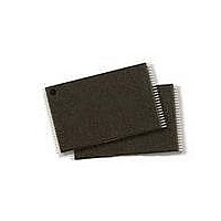
S29JL064H70TFI000 Spansion Inc., S29JL064H70TFI000 Datasheet - Page 15

S29JL064H70TFI000
Manufacturer Part Number
S29JL064H70TFI000
Description
IC, FLASH, 64MBIT, 70NS, TSOP-48
Manufacturer
Spansion Inc.
Datasheet
1.S29JL064H90TFI000.pdf
(61 pages)
Specifications of S29JL064H70TFI000
Memory Type
Flash
Memory Size
64Mbit
Memory Configuration
8M X 8 / 4M X 16
Ic Interface Type
CFI, Parallel
Access Time
70ns
Supply Voltage Range
2.7 To 3.6 V
Memory Case Style
TSOP
Data Bus Width
8 bit, 16 bit
Architecture
Boot Sector
Interface Type
Conventional
Supply Voltage (max)
3.6 V
Supply Voltage (min)
2.7 V
Maximum Operating Current
10 mA
Mounting Style
SMD/SMT
Operating Temperature
+ 85 C
Package / Case
TSOP-48
Lead Free Status / RoHS Status
Lead free / RoHS Compliant
Lead Free Status / RoHS Status
Lead free / RoHS Compliant, Lead free / RoHS Compliant
Available stocks
Company
Part Number
Manufacturer
Quantity
Price
Part Number:
S29JL064H70TFI000
Manufacturer:
PANSION
Quantity:
20 000
Company:
Part Number:
S29JL064H70TFI000H
Manufacturer:
SPANSION
Quantity:
121
8.2
8.3
September 8, 2009 S29JL064H_00_A8
8.3.1
8.3.2
Requirements for Reading Array Data
Writing Commands/Command Sequences
Accelerated Program Operation
Autoselect Functions
To read array data from the outputs, the system must drive the CE# and OE# pins to V
control and selects the device. OE# is the output control and gates array data to the output pins. WE# should
remain at V
The internal state machine is set for reading array data upon device power-up, or after a hardware reset. This
ensures that no spurious alteration of the memory content occurs during the power transition. No command is
necessary in this mode to obtain array data. Standard microprocessor read cycles that assert valid addresses
on the device address inputs produce valid data on the device data outputs. Each bank remains enabled for
read access until the command register contents are altered.
Refer to
timing diagram. I
array data.
To write a command or command sequence (which includes programming data to the device and erasing
sectors of memory), the system must drive WE# and CE# to V
For program operations, the BYTE# pin determines whether the device accepts program data in bytes or
words. Refer to
The device features an Unlock Bypass mode to facilitate faster programming. Once a bank enters the
Unlock Bypass mode, only two write cycles are required to program a word or byte, instead of four.
Word Program Command Sequence on page 32
standard and Unlock Bypass command sequences.
An erase operation can erase one sector, multiple sectors, or the entire device.
indicates the address space that each sector occupies. Similarly, a sector address is the address bits
required to uniquely select a sector.
entire chip, or suspending/resuming the erase operation.
The device address space is divided into four banks. A bank address is the address bits required to uniquely
select a bank.
I
Characteristics on page 46
The device offers accelerated program operations through the ACC function. This is one of two functions
provided by the WP#/ACC pin. This function is primarily intended to allow faster manufacturing throughput at
the factory.
If the system asserts V
mode, temporarily unprotects any protected sectors, and uses the higher voltage on the pin to reduce the
time required for program operations. The system would use a two-cycle program command sequence as
required by the Unlock Bypass mode. Removing V
operation. Note that V
programming, or device damage may result. In addition, the WP#/ACC pin must not be left floating or
unconnected; inconsistent behavior of the device may result.
information.
If the system writes the autoselect command sequence, the device enters the autoselect mode. The system
can then read autoselect codes from the internal register (which is separate from the memory array) on
DQ15–DQ0. Standard read cycle timings apply in this mode. Refer to
Autoselect Command Sequence on page 32
CC2
in the
Read-Only Operations on page 46
DC Characteristics on page 43
IH
. The BYTE# pin determines whether the device outputs array data in words or bytes.
Word/Byte Configuration on page 14
CC1
in
HH
HH
DC Characteristics on page 43
D a t a
must not be asserted on WP#/ACC for operations other than accelerated
on this pin, the device automatically enters the aforementioned Unlock Bypass
contains timing specification tables and timing diagrams for write operations.
S h e e t
Command Definitions on page 31
S29JL064H
represents the active current specification for the write mode.
for timing specifications and to
for more information.
has details on programming data to the device using both
HH
for more information.
from the WP#/ACC pin returns the device to normal
represents the active current specification for reading
Write Protect (WP#) on page 23
IL
, and OE# to V
Autoselect Mode on page 21
has details on erasing a sector or the
Figure 17.1 on page 46
IH
Table 8.3 on page 20
.
IL
. CE# is the power
for related
for the
Byte/
and
AC
15


