S29JL064H70TFI000 Spansion Inc., S29JL064H70TFI000 Datasheet - Page 27

S29JL064H70TFI000
Manufacturer Part Number
S29JL064H70TFI000
Description
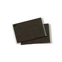
IC, FLASH, 64MBIT, 70NS, TSOP-48
Manufacturer
Spansion Inc.
Datasheet
1.S29JL064H90TFI000.pdf
(61 pages)
Specifications of S29JL064H70TFI000
Memory Type
Flash
Memory Size
64Mbit
Memory Configuration
8M X 8 / 4M X 16
Ic Interface Type
CFI, Parallel
Access Time
70ns
Supply Voltage Range
2.7 To 3.6 V
Memory Case Style
TSOP
Data Bus Width
8 bit, 16 bit
Architecture
Boot Sector
Interface Type
Conventional
Supply Voltage (max)
3.6 V
Supply Voltage (min)
2.7 V
Maximum Operating Current
10 mA
Mounting Style
SMD/SMT
Operating Temperature
+ 85 C
Package / Case
TSOP-48
Lead Free Status / RoHS Status
Lead free / RoHS Compliant
Lead Free Status / RoHS Status
Lead free / RoHS Compliant, Lead free / RoHS Compliant
Available stocks
Company
Part Number
Manufacturer
Quantity
Price
Part Number:
S29JL064H70TFI000
Manufacturer:
PANSION
Quantity:
20 000
Company:
Part Number:
S29JL064H70TFI000H
Manufacturer:
SPANSION
Quantity:
121
8.14
September 8, 2009 S29JL064H_00_A8
8.14.1
8.14.2
8.14.3
8.14.4
Hardware Data Protection
Low V
Write Pulse Glitch Protection
Logical Inhibit
Power-Up Write Inhibit
The Secured Silicon Sector lock must be used with caution since, once locked, there is no procedure
available for unlocking the Secured Silicon Sector area and none of the bits in the Secured Silicon Sector
memory space can be modified in any way.
The command sequence requirement of unlock cycles for programming or erasing provides data protection
against inadvertent writes (refer to
hardware data protection measures prevent accidental erasure or programming, which might otherwise be
caused by spurious system level signals during V
noise.
When V
power-up and power-down. The command register and all internal program/erase circuits are disabled, and
the device resets to the read mode. Subsequent writes are ignored until V
system must provide the proper signals to the control pins to prevent unintentional writes when V
than V
Noise pulses of less than 5 ns (typical) on OE#, CE# or WE# do not initiate a write cycle.
Write cycles are inhibited by holding any one of OE# = V
CE# and WE# must be a logical zero while OE# is a logical one.
If WE# = CE# = V
edge of WE#. The internal state machine is automatically reset to the read mode on power-up.
LKO
CC
CC
.
Write Inhibit
is less than V
IL
and OE# = V
LKO
D a t a
, the device does not accept any write cycles. This protects data during V
Figure 8.3 Secured Silicon Sector Protect Verify
IH
Table 10.1 on page 36
S h e e t
Silicon Sector address
Silicon Sector address
during power up, the device does not accept commands on the rising
Write 40h to Secure
Read from Secure
A1 = 1, A0 = 0
A1 = 1, A0 = 0
Write 60h to
any address
with A6 = 0,
with A6 = 0,
RESET# =
S29JL064H
Wait 1 ms
V
START
IH
or V
ID
CC
power-up and power-down transitions, or from system
IL
Secure Silicon Sector
Secure Silicon Sector
Secure Silicon Sector
Remove V
for command definitions). In addition, the following
, CE# = V
If data = 00h,
is unprotected.
If data = 01h,
from RESET#
Protect Verify
is protected.
Write reset
command
complete
IH
IH
or V
or WE# = V
ID
CC
is greater than V
IH
. To initiate a write cycle,
LKO
CC
. The
is greater
CC
27


