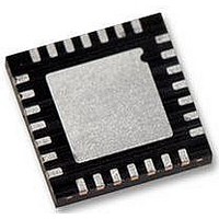
PIC16F1827-I/MQ Microchip Technology, PIC16F1827-I/MQ Datasheet - Page 204

PIC16F1827-I/MQ
Manufacturer Part Number
PIC16F1827-I/MQ
Description
IC, 8BIT MCU, PIC16F, 32MHZ, QFN-28
Manufacturer
Microchip Technology
Datasheet
1.PIC16LF1827-ISS.pdf
(400 pages)
Specifications of PIC16F1827-I/MQ
Controller Family/series
PIC16F
Eeprom Memory Size
256Byte
Ram Memory Size
384Byte
Cpu Speed
32MHz
No. Of Timers
5
Interface
EUSART, I2C, SPI
Core Size
8 Bit
Program Memory Size
4 Kwords
Processor Series
PIC16F
Core
PIC
Data Bus Width
8 bit
Program Memory Type
Flash
Data Ram Size
384 B
Interface Type
I2C, SPI, UART
Maximum Clock Frequency
32 MHz
Number Of Programmable I/os
15
Number Of Timers
5
Maximum Operating Temperature
+ 85 C
Mounting Style
SMD/SMT
Package / Case
QFN EP
3rd Party Development Tools
52715-96, 52716-328, 52717-734
Development Tools By Supplier
PG164130, DV164035, DV244005, DV164005
Minimum Operating Temperature
- 40 C
On-chip Adc
10 bit, 12 Channel
Lead Free Status / Rohs Status
Details
- Current page: 204 of 400
- Download datasheet (7Mb)
PIC16F/LF1826/27
23.1
The Capture/Compare/PWM module is a peripheral
which allows the user to time and control different
events. In Capture mode, the peripheral allows the
timing of the duration of an event. The Compare mode
allows the user to trigger an external event when a
predetermined amount of time has expired. The PWM
mode can generate a Pulse-Width Modulated signal of
varying frequency and duty cycle.
Table 23-1 shows the timer resources required by the
CCP module.
REGISTER 23-1:
DS41391B-page 204
bit 7
Legend:
R = Readable bit
u = Bit is unchanged
‘1’ = Bit is set
bit 7-6
bit 5-4
R/W-0/0
PxM1
Capture/Compare/PWM
(1)
PxM<1:0>: Enhanced PWM Output Configuration bits
If CCPxM<3:2> = 00, 01, 10:
xx = PxA assigned as Capture/Compare input; PxB, PxC, PxD assigned as port pins
If CCPxM<3:2> = 11:
00 = Single output; PxA modulated; PxB, PxC, PxD assigned as port pins
01 = Full-Bridge output forward; P1D modulated; P1A active; P1B, P1C inactive
10 = Half-Bridge output; P1A, P1B modulated with dead-band control; P1C, P1D assigned as port pins
11 = Full-Bridge output reverse; P1B modulated; P1C active; P1A, P1D inactive
DCxB<1:0>: PWM Duty Cycle Least Significant bits
Capture mode:
Unused
Compare mode:
Unused
PWM mode:
These bits are the two LSbs of the PWM duty cycle. The eight MSbs are found in CCPRxL.
R/W-0/0
PxM0
CCPXCON: CCPX CONTROL REGISTER
(1)
W = Writable bit
x = Bit is unknown
‘0’ = Bit is cleared
R/W-0/0
DCxB1
R/W-0/0
DCxB0
Preliminary
U = Unimplemented bit, read as ‘0’
-n/n = Value at POR and BOR/Value at all other Reset
CCPxM3
R/W-0/0
TABLE 23-1:
(1)
CCP Mode
Compare
Capture
PWM
CCPxM2
R/W-0/0
REQUIRED TIMER
RESOURCES
© 2009 Microchip Technology Inc.
CCPxM1
R/W-0/0
Timer Resource
Timer2 or 4 or 6
Timer1
Timer1
CCPxM0
R/W-0/0
bit 0
Related parts for PIC16F1827-I/MQ
Image
Part Number
Description
Manufacturer
Datasheet
Request
R

Part Number:
Description:
IC, 8BIT MCU, PIC16F, 32MHZ, SOIC-18
Manufacturer:
Microchip Technology
Datasheet:

Part Number:
Description:
IC, 8BIT MCU, PIC16F, 32MHZ, SSOP-20
Manufacturer:
Microchip Technology
Datasheet:

Part Number:
Description:
IC, 8BIT MCU, PIC16F, 32MHZ, DIP-18
Manufacturer:
Microchip Technology
Datasheet:

Part Number:
Description:
IC, 8BIT MCU, PIC16F, 32MHZ, QFN-28
Manufacturer:
Microchip Technology
Datasheet:

Part Number:
Description:
IC, 8BIT MCU, PIC16F, 32MHZ, QFN-28
Manufacturer:
Microchip Technology
Datasheet:

Part Number:
Description:
IC, 8BIT MCU, PIC16F, 32MHZ, QFN-28
Manufacturer:
Microchip Technology
Datasheet:

Part Number:
Description:
IC, 8BIT MCU, PIC16F, 32MHZ, SSOP-20
Manufacturer:
Microchip Technology
Datasheet:

Part Number:
Description:
IC, 8BIT MCU, PIC16F, 20MHZ, DIP-40
Manufacturer:
Microchip Technology
Datasheet:

Part Number:
Description:
IC, 8BIT MCU, PIC16F, 20MHZ, MQFP-44
Manufacturer:
Microchip Technology
Datasheet:

Part Number:
Description:
IC, 8BIT MCU, PIC16F, 20MHZ, QFN-20
Manufacturer:
Microchip Technology
Datasheet:

Part Number:
Description:
IC, 8BIT MCU, PIC16F, 32MHZ, QFN-28
Manufacturer:
Microchip Technology
Datasheet:

Part Number:
Description:
MCU 14KB FLASH 768B RAM 64-TQFP
Manufacturer:
Microchip Technology
Datasheet:

Part Number:
Description:
7 KB Flash, 384 Bytes RAM, 32 MHz Int. Osc, 16 I/0, Enhanced Mid Range Core, Low
Manufacturer:
Microchip Technology

Part Number:
Description:
14KB Flash, 512B RAM, 256B EEPROM, LCD, 1.8-5.5V 40 UQFN 5x5x0.5mm TUBE
Manufacturer:
Microchip Technology
Datasheet:

Part Number:
Description:
14KB Flash, 512B RAM, 256B EEPROM, LCD, 1.8-5.5V 40 UQFN 5x5x0.5mm TUBE
Manufacturer:
Microchip Technology


