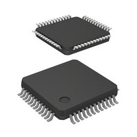
LPC1225FBD48/321 NXP Semiconductors, LPC1225FBD48/321 Datasheet - Page 20

LPC1225FBD48/321
Manufacturer Part Number
LPC1225FBD48/321
Description
MCU, 80K FLASH, CORTEX-M0, 48LQFP
Manufacturer
NXP Semiconductors
Datasheet
1.LPC1224FBD48201.pdf
(60 pages)
Specifications of LPC1225FBD48/321
Rohs Compliant
YES
Featured Product
LPC122x Cortex-M0 Microcontrollers
Core Processor
ARM Cortex-M0
Core Size
32-Bit
Speed
45MHz
Connectivity
I²C, IrDA, Microwire, SPI, SSI, SSP, UART/USART
Peripherals
Brown-out Detect/Reset, DMA, POR, WDT
Number Of I /o
39
Program Memory Size
80KB (80K x 8)
Program Memory Type
FLASH
Ram Size
8K x 8
Voltage - Supply (vcc/vdd)
3 V ~ 3.6 V
Data Converters
A/D 8x10b
Oscillator Type
Internal
Operating Temperature
-40°C ~ 85°C
Package / Case
48-LQFP
Controller Family/series
LPC1200
No. Of I/o's
39
Ram Memory Size
8KB
Cpu Speed
30MHz
No. Of Timers
4
Lead Free Status / RoHS Status
Lead free / RoHS Compliant
Other names
568-5158
LPC1225FBD48/321
LPC1225FBD48/321
Available stocks
Company
Part Number
Manufacturer
Quantity
Price
Company:
Part Number:
LPC1225FBD48/321
Manufacturer:
NXP
Quantity:
2 000
Part Number:
LPC1225FBD48/321
Manufacturer:
NXP/恩智浦
Quantity:
20 000
Company:
Part Number:
LPC1225FBD48/321,1
Manufacturer:
NXP Semiconductors
Quantity:
10 000
NXP Semiconductors
LPC122X
Objective data sheet
7.10.1 Features
7.12.1 Features
7.11.1 Features
7.12 I
7.11 SSP/SPI serial I/O controller
The LPC122x contain one SSP/SPI controller. The SSP/SPI controller is capable of
operation on a SSP, 4-wire SSI, or Microwire bus. It can interact with multiple masters and
slaves on the bus. Only a single master and a single slave can communicate on the bus
during a given data transfer. The SSP supports full duplex transfers, with frames of 4 bits
to 16 bits of data flowing from the master to the slave and from the slave to the master. In
practice, often only one of these data flows carries meaningful data.
The LPC122x contain one I
The I
(SCL) and a serial data line (SDA). Each device is recognized by a unique address and
can operate as either a receiver-only device (e.g., an LCD driver) or a transmitter with the
capability to both receive and send information (such as memory). Transmitters and/or
receivers can operate in either master or slave mode, depending on whether the chip has
to initiate a data transfer or is only addressed. The I
controlled by more than one bus master connected to it.
2
•
•
•
•
•
•
•
•
•
•
•
•
•
•
•
•
C-bus serial I/O controller
16-byte Receive and Transmit FIFOs.
Register locations conform to 16C550 industry standard.
Receiver FIFO trigger points at 1 B, 4 B, 8 B, and 14 B.
Built-in fractional baud rate generator covering wide range of baud rates without a
need for external crystals of particular values.
Auto-baud capabilities and FIFO control mechanism that enables software flow
control implementation.
Support for RS-485/9-bit mode (UART0).
Support for modem control (UART0).
Compatible with Motorola SPI, 4-wire Texas Instruments SSI, and National
Semiconductor Microwire buses
Synchronous serial communication
Master or slave operation
8-frame FIFOs for both transmit and receive
4-bit to 16-bit frame
The I
supports I
Programmable digital glitch filter providing a 60 ns to 1 s input filter.
Easy to configure as master, slave, or master/slave.
Programmable clocks allow versatile rate control.
2
C-bus is bidirectional for inter-IC control using only two wires: a serial clock line
2
C-interface is a standard I
2
C Fast-mode Plus with bit rates of up to 1 Mbit/s.
All information provided in this document is subject to legal disclaimers.
Rev. 1.2 — 29 March 2011
2
C-bus controller.
2
C-compliant bus interface with open-drain pins and
32-bit ARM Cortex-M0 microcontroller
2
C is a multi-master bus and can be
LPC122x
© NXP B.V. 2011. All rights reserved.
20 of 60


