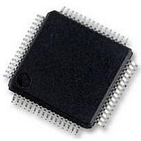
LPC2119FBD64 NXP Semiconductors, LPC2119FBD64 Datasheet - Page 14

LPC2119FBD64
Manufacturer Part Number
LPC2119FBD64
Description
16/32BIT MCU ARM7, 128K FLASH, 64LQFP
Manufacturer
NXP Semiconductors
Datasheet
1.LPC2119FBD64.pdf
(44 pages)
Specifications of LPC2119FBD64
No. Of I/o's
46
Ram Memory Size
16KB
Cpu Speed
60MHz
No. Of Timers
2
No. Of Pwm Channels
6
Digital Ic Case
RoHS Compliant
Core Size
32bit
Program Memory Size
128KB
Oscillator Type
External Only
Controller Family/series
LPC21xx
Rohs Compliant
Yes
Data Bus Width
16 bit, 32 bit
Program Memory Type
Flash
Data Ram Size
16 KB
Interface Type
CAN, I2C, JTAG, SPI, SSP, UART
Maximum Clock Frequency
60 MHz
Number Of Programmable I/os
46
Number Of Timers
2
Maximum Operating Temperature
+ 85 C
Mounting Style
SMD/SMT
Package / Case
LQFP
Minimum Operating Temperature
- 40 C
On-chip Adc
10 bit, 4 Channel
Lead Free Status / Rohs Status
Details
Available stocks
Company
Part Number
Manufacturer
Quantity
Price
Company:
Part Number:
LPC2119FBD64
Manufacturer:
NXP
Quantity:
5 000
Company:
Part Number:
LPC2119FBD64
Manufacturer:
NXP
Quantity:
748
Part Number:
LPC2119FBD64
Manufacturer:
NXP/恩智浦
Quantity:
20 000
Company:
Part Number:
LPC2119FBD64,151
Manufacturer:
NXP Semiconductors
Quantity:
10 000
Company:
Part Number:
LPC2119FBD64/01
Manufacturer:
NXP
Quantity:
8 000
Company:
Part Number:
LPC2119FBD64/01,15
Manufacturer:
Maxim
Quantity:
93
Company:
Part Number:
LPC2119FBD64/01,15
Manufacturer:
NXP Semiconductors
Quantity:
10 000
NXP Semiconductors
Product data sheet
LPC2109_2119_2129_6
6.7.1 Features
6.7.2 Features added with the Fast GPIO set of registers available on
6.6 Pin connect block
6.7 General purpose parallel I/O (GPIO) and Fast I/O
Table 4.
[1]
The pin connect block allows selected pins of the microcontroller to have more than one
function. Configuration registers control the multiplexers to allow connection between the
pin and the on-chip peripherals. Peripherals should be connected to the appropriate pins
prior to being activated, and prior to any related interrupt(s) being enabled. Activity of any
enabled peripheral function that is not mapped to a related pin should be considered
undefined.
Device pins that are not connected to a specific peripheral function are controlled by the
parallel I/O registers. Pins may be dynamically configured as inputs or outputs. Separate
registers allow setting or clearing any number of outputs simultaneously. The value of the
output register may be read back, as well as the current state of the port pins.
LPC2109/2119/2129/01 only
Block
System Control
ADC
CAN
•
•
•
•
•
•
•
•
•
SSP interface available on LPC2109/01, LPC2119/01, and LPC2129/01 only.
Bit-level set and clear registers allow a single instruction set or clear of any number of
bits in one port.
Direction control of individual bits.
Separate control of output set and clear.
All I/O default to inputs after reset.
Fast GPIO registers are relocated to the ARM local bus for the fastest possible I/O
timing, enabling port pin toggling up to 3.5 times faster than earlier LPC2000 devices.
Mask registers allow treating sets of port bits as a group, leaving other bits
unchanged.
All Fast GPIO registers are byte addressable.
Entire port value can be written in one instruction.
Ports are accessible via either the legacy group of registers (GPIOs) or the group of
registers providing accelerated port access (Fast GPIOs).
Interrupt sources
Flag(s)
External Interrupt 0 (EINT0)
External Interrupt 1 (EINT1)
External Interrupt 2 (EINT2)
External Interrupt 3 (EINT3)
A/D Converter
CAN1, CAN2 and Acceptance Filter
Rev. 06 — 10 December 2007
…continued
LPC2109/2119/2129
Single-chip 16/32-bit microcontrollers
© NXP B.V. 2007. All rights reserved.
VIC channel #
14
15
16
17
18
19 to 23
14 of 44


