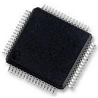
LPC2119FBD64 NXP Semiconductors, LPC2119FBD64 Datasheet - Page 15

LPC2119FBD64
Manufacturer Part Number
LPC2119FBD64
Description
16/32BIT MCU ARM7, 128K FLASH, 64LQFP
Manufacturer
NXP Semiconductors
Datasheet
1.LPC2119FBD64.pdf
(44 pages)
Specifications of LPC2119FBD64
No. Of I/o's
46
Ram Memory Size
16KB
Cpu Speed
60MHz
No. Of Timers
2
No. Of Pwm Channels
6
Digital Ic Case
RoHS Compliant
Core Size
32bit
Program Memory Size
128KB
Oscillator Type
External Only
Controller Family/series
LPC21xx
Rohs Compliant
Yes
Data Bus Width
16 bit, 32 bit
Program Memory Type
Flash
Data Ram Size
16 KB
Interface Type
CAN, I2C, JTAG, SPI, SSP, UART
Maximum Clock Frequency
60 MHz
Number Of Programmable I/os
46
Number Of Timers
2
Maximum Operating Temperature
+ 85 C
Mounting Style
SMD/SMT
Package / Case
LQFP
Minimum Operating Temperature
- 40 C
On-chip Adc
10 bit, 4 Channel
Lead Free Status / Rohs Status
Details
Available stocks
Company
Part Number
Manufacturer
Quantity
Price
Company:
Part Number:
LPC2119FBD64
Manufacturer:
NXP
Quantity:
5 000
Company:
Part Number:
LPC2119FBD64
Manufacturer:
NXP
Quantity:
748
Part Number:
LPC2119FBD64
Manufacturer:
NXP/恩智浦
Quantity:
20 000
Company:
Part Number:
LPC2119FBD64,151
Manufacturer:
NXP Semiconductors
Quantity:
10 000
Company:
Part Number:
LPC2119FBD64/01
Manufacturer:
NXP
Quantity:
8 000
Company:
Part Number:
LPC2119FBD64/01,15
Manufacturer:
Maxim
Quantity:
93
Company:
Part Number:
LPC2119FBD64/01,15
Manufacturer:
NXP Semiconductors
Quantity:
10 000
NXP Semiconductors
Product data sheet
LPC2109_2119_2129_6
6.10.1 Features
6.8.1 Features
6.8.2 ADC features available in LPC2109/2119/2129/01 only
6.9.1 Features
6.10 UARTs
6.8 10-bit ADC
6.9 CAN controllers and acceptance filter
The LPC2109/2119/2129 each contain a single 10-bit successive approximation ADC with
four multiplexed channels.
The LPC2119 and LPC2129 each contain two CAN controllers, while the LPC2109 has
one CAN controller. The CAN is a serial communications protocol which efficiently
supports distributed real-time control with a very high level of security. Its domain of
application ranges from high-speed networks to low-cost multiplex wiring.
The LPC2109/2119/2129 each contain two UARTs. In addition to standard transmit and
receive data lines, the UART1 also provides a full modem control handshake interface.
•
•
•
•
•
•
•
•
•
•
•
•
•
•
•
•
•
Measurement range of 0 V to 3 V.
Capable of performing more than 400000 10-bit samples per second.
Burst conversion mode for single or multiple inputs.
Optional conversion on transition on input pin or Timer Match signal.
Every analog input has a dedicated result register to reduce interrupt overhead.
Every analog input can generate an interrupt once the conversion is completed.
The ADC pads are 5 V tolerant when configured for digital I/O function(s).
Data rates up to 1 Mbit/s on each bus.
32-bit register and RAM access.
Compatible with CAN specification 2.0B, ISO 11898-1.
Global Acceptance Filter recognizes 11-bit and 29-bit Rx identifiers for all CAN buses.
Acceptance Filter can provide FullCAN-style automatic reception for selected
Standard identifiers.
16 B Receive and Transmit FIFOs.
Register locations conform to 16C550 industry standard.
Receiver FIFO trigger points at 1 B, 4 B, 8 B, and 14 B.
Built-in fractional baud rate generator covering wide range of baud rates without a
need for external crystals of particular values.
Transmission FIFO control enables implementation of software (XON/XOFF) flow
control on both UARTs.
Rev. 06 — 10 December 2007
LPC2109/2119/2129
Single-chip 16/32-bit microcontrollers
© NXP B.V. 2007. All rights reserved.
15 of 44


