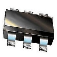
LTC3525ESC6-3#PBF Linear Technology, LTC3525ESC6-3#PBF Datasheet - Page 3

LTC3525ESC6-3#PBF
Manufacturer Part Number
LTC3525ESC6-3#PBF
Description
IC, SYNC STEP-UP DC/DC CONVERTER, SC70-6
Manufacturer
Linear Technology
Datasheet
1.LTC3525ESC6-3PBF.pdf
(14 pages)
Specifications of LTC3525ESC6-3#PBF
Primary Input Voltage
1.2V
No. Of Outputs
1
Output Voltage
3V
Output Current
400mA
No. Of Pins
6
Operating Temperature Range
-40°C To +85°C
Termination Type
SMD
Msl
MSL 1 - Unlimited
Rohs Compliant
Yes
Lead Free Status / RoHS Status
Lead free / RoHS Compliant
Available stocks
Company
Part Number
Manufacturer
Quantity
Price
ELECTRICAL CHARACTERISTICS
The
V
PARAMETER
Input Start-Up Voltage
Output Voltage
Quiescent Current, V
Quiescent Current, V
Quiescent Current, V
NMOS Switch Leakage Current
PMOS Switch Leakage Current
NMOS Switch On-Resistance
PMOS Switch On-Resistance
Peak Current Limit
SHDN Threshold Voltage
SHDN Input Current
(LTC3525-5)
The
V
PARAMETER
Input Start-Up Voltage
Output Voltage
Quiescent Current, V
Quiescent Current, V
Quiescent Current, V
NMOS Switch Leakage Current
PMOS Switch Leakage Current
NMOS Switch On-Resistance
PMOS Switch On-Resistance
Peak Current Limit
SHDN Threshold Voltage
SHDN Input Current
Note 1: Stresses beyond those listed under Absolute Maximum Ratings
may cause permanent damage to the device. Exposure to any Absolute
Maximum Rating condition for extended periods may affect device
reliability and lifetime.
Note 2: The LTC3525E is guaranteed to meet performance specifications
from 0°C to 85°C. Specifications over the –40°C to 85°C operating
temperature range are assured by design, characterization and correlation
with statistical process controls.
Note 3: Specification is guaranteed by design and not 100% tested in
production.
IN
IN
= 1.2V, V
= 2.4V, V
l
l
denotes the specifications which apply over the full operating temperature range, otherwise specifications are at T
denotes the specifications which apply over the full operating temperature range, otherwise specifications are at T
SHDN
SHDN
= 1.2V, V
= 2.4V, V
OUT
IN
IN
OUT
IN
IN
– Shutdown
– Shutdown
OUT
OUT
= 3.3V unless otherwise noted.
= 5V unless otherwise noted.
CONDITIONS
CONDITIONS
(Note 6)
SHDN = V
SHDN = V
SHDN = 0V, V
Not Including Switch Leakage
V
V
(Note 3)
(Note 3)
V
(Note 6)
SHDN = V
SHDN = V
SHDN = 0V, V
Not Including Switch Leakage
V
V
(Note 3)
(Note 3)
V
IN
IN
SHDN
IN
IN
SHDN
= V
= V
= V
= V
= V
= V
OUT
SW
OUT
SW
IN
IN
IN
IN
IN
IN
= 5V, V
= 5V, V
= V
= V
(LTC3525-3.3)
(Note 4)
(Note 4)
(Note 4)
(Note 4)
or V
or V
OUT
OUT
SW
SW
OUT
OUT
OUT
OUT
= 0V
= 0V
= 5V, SHDN = 0V
= 5V, SHDN = 0V
= 0V, SHDN = 0V
= 0V, SHDN = 0V
Note 4: Current Measurements are performed when the LTC3525 is not
switching.
Note 5: This IC includes overtemperature protection that is intended
to protect the device during momentary overload conditions. Junction
temperature will exceed 125°C when overtemperature protection is active.
Continuous operation above the specified maximum operating junction
temperature may impair device reliability.
Note 6: Consult LTC Marketing for other output voltage options.
LTC3525-3.3/LTC3525-5
l
l
MIN
3.20
MIN
4.85
0.4
0.4
0.4
0.4
LTC3525-3/
0.85
3.30
0.45
0.01
0.85
5.00
0.01
TYP
TYP
0.5
0.1
0.1
0.1
0.5
0.8
0.6
1.5
0.1
0.1
0.1
0.4
0.7
0.5
0.6
7
8
MAX
MAX
3.40
5.15
15
18
A
A
1
3
1
1
3
1
1
1
5
1
1
3
1
1
= 25°C.
= 25°C.
UNITS
UNITS
3525fb
3
µA
µA
µA
µA
µA
µA
µA
µA
µA
µA
µA
µA
Ω
Ω
Ω
Ω
V
V
A
V
V
V
A
V


