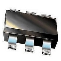
LTC3525ESC6-3#PBF Linear Technology, LTC3525ESC6-3#PBF Datasheet - Page 7

LTC3525ESC6-3#PBF
Manufacturer Part Number
LTC3525ESC6-3#PBF
Description
IC, SYNC STEP-UP DC/DC CONVERTER, SC70-6
Manufacturer
Linear Technology
Datasheet
1.LTC3525ESC6-3PBF.pdf
(14 pages)
Specifications of LTC3525ESC6-3#PBF
Primary Input Voltage
1.2V
No. Of Outputs
1
Output Voltage
3V
Output Current
400mA
No. Of Pins
6
Operating Temperature Range
-40°C To +85°C
Termination Type
SMD
Msl
MSL 1 - Unlimited
Rohs Compliant
Yes
Lead Free Status / RoHS Status
Lead free / RoHS Compliant
Available stocks
Company
Part Number
Manufacturer
Quantity
Price
PIN FUNCTIONS
SHDN (Pin 1): Logic-Controlled Shutdown Input. Con-
nect to a voltage >1V to enable the LTC3525. Connect to
a voltage <0.4V to disable the LTC3525.
GND (Pins 2, 5): Ground.
V
V
+ 0.2V typical), it is powered from V
bypass capacitor from V
1µF is recommended.
BLOCK DIAGRAM
IN
IN
until V
(Pin 3): Input Voltage. The LTC3525 is powered from
SHDN
OUT
1
exceeds V
SHUTDOWN
SHUTDOWN
V
THERMAL
OUT
V
UVLO
V
BEST
REF
IN
IN
SHUTDOWN
START-UP
. Once V
to GND. A minimum value of
VB
SHUTDOWN
V
REF
TSD
UVLO
V
SEL
OUT
OUT
is greater than (V
GATE DRIVERS
CONDUCTION
ANTI-CROSS
. Place a ceramic
LOGIC
AND
GND
5
I
PK
I
VAL
WAKE
SW
COMPARATOR
IN
6
GND
INTEGRATOR
–
+
2
I
PK
ADJUST
OFFSET
V
Synchronous Rectifier. Connect the output filter capacitor
from V
10µF ceramic is recommended. Use 22µF for reduced
output ripple. The output disconnect feature disconnects
V
SW (Pin 6): Switch Pin. Connect an inductor from this
pin to V
across SW and V
to zero to minimize EMI.
COMPARATOR
OUT
OUT
I
VALLEY
–
+
(Pin 4): Output Voltage Sense and the Output of the
from V
+
–
OUT
ADJUST
IN
LTC3525-3.3/LTC3525-5
COMPARATOR
. An internal antiringing resistor is connected
to GND, close to the IC. A minimum value of
SLEEP
IN
–
+
OFFSET
when SHDN is <0.4V.
IN
V
REF
after the inductor current has dropped
FB
+
–
ADJUST
SWITCH
WELL
V
3
IN
LTC3525-3/
3525 BD
4
V
OUT
3525fb
7


