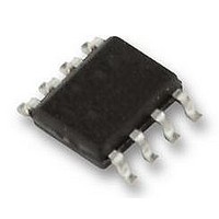
LP2996MR National Semiconductor, LP2996MR Datasheet - Page 13

LP2996MR
Manufacturer Part Number
LP2996MR
Description
IC, REG DDR TERMINATION, SMD, PSOP8
Manufacturer
National Semiconductor
Datasheet
1.LP2996M.pdf
(18 pages)
Specifications of LP2996MR
Primary Input Voltage
2.5V
Output Voltage
1.35V
No. Of Pins
8
Output Current
1.5A
Voltage Regulator Case Style
PSOP
Operating Temperature Range
0°C To +125°C
Svhc
No SVHC (15-Dec-2010)
Output Voltage Fixed
1.35V
Rohs Compliant
Yes
No. Of Outputs
1
Filter Terminals
SMD
Mounting Type
Surface Mount
Input Voltage Primary Max
5V
Lead Free Status / RoHS Status
Lead free / RoHS Compliant
Available stocks
Company
Part Number
Manufacturer
Quantity
Price
Company:
Part Number:
LP2996MR
Manufacturer:
ns
Quantity:
2 560
Part Number:
LP2996MR
Manufacturer:
NS/国半
Quantity:
20 000
Company:
Part Number:
LP2996MR/NOPB
Manufacturer:
SANYO
Quantity:
195
Part Number:
LP2996MR/NOPB
Manufacturer:
NS/国半
Quantity:
20 000
Company:
Part Number:
LP2996MRX
Manufacturer:
TI
Quantity:
6 222
Part Number:
LP2996MRX
Manufacturer:
NS/国半
Quantity:
20 000
Company:
Part Number:
LP2996MRX/NOPB
Manufacturer:
NS
Quantity:
16 701
Part Number:
LP2996MRX/NOPB
Manufacturer:
TI/德州仪器
Quantity:
20 000
Company:
Part Number:
LP2996MRX_NOPB
Manufacturer:
National
Quantity:
1 245
LEVEL SHIFTING
If standards other than SSTL-2 are required, such as SSTL-3,
it may be necessary to use a different scaling factor than 0.5
times V
are available to scale the output to any voltage required. One
method is to level shift the output by using feedback resistors
Conversely, the R2 resistor can be placed between V
and V
ence voltage of VDDQ/2. The equations relating VTT and the
resistors can be seen below:
HSTL APPLICATIONS
The LP2996 can be easily adapted for HSTL applications by
connecting V
DDQ
DDQ
to shift the V
for regulating the output voltage. Several options
DDQ
to the 1.5V rail. This will produce a V
TT
output lower than the internal refer-
FIGURE 11. Decreasing VTT by Level Shifting
FIGURE 10. Increasing VTT by Level Shifting
FIGURE 12. HSTL Application
TT
SENSE
and
13
from V
10 and 11. Figure 10 shows how to use two resistors to level
shift V
calculate the exact voltage at V
be used.
V
sistors. AVIN and PVIN should be connected to a 2.5V rail for
optimal performance.
REF
voltage of approximately 0.75V for the termination re-
TT
TT
to the V
above the internal reference voltage of VDDQ/2. To
SENSE
V
V
TT
TT
= VDDQ/2 ( 1 + R1/R2)
= VDDQ/2 (1 - R1/R2)
20057516
pin. This has been illustrated in Figures
20057515
20057517
TT
the following equation can
www.national.com


