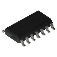
HFA3600IB Intersil, HFA3600IB Datasheet - Page 12

HFA3600IB
Manufacturer Part Number
HFA3600IB
Description
IC, LOW-NOISE AMP, 19.8DB 900MHZ SOIC-14
Manufacturer
Intersil
Datasheet
1.HFA3600IB.pdf
(16 pages)
Specifications of HFA3600IB
Frequency Range
900MHz
Noise Figure Typ
3.97dB
Power Dissipation Pd
1W
Supply Current
11.3mA
Supply Voltage Range
4V To 5.5V
Gain
19.8dB
Rf Type
Cellular, GSM, ISM, PCS
Lead Free Status / RoHS Status
Contains lead / RoHS non-compliant
Pin Description
LNA V
Supply voltage for the Low Noise amplifier.
LNA In
LNA input. Requires AC coupling. Minimum coupling
capacitor value of 100pF is suggested. This input is
optimized for 50W match in the 800MHz to 1000MHz range.
LO Bypass
Mixer LO Bypass. Capacitor required to assure a good AC
ground. Placement is critical. The bypass capacitance
should be located close to the device with low ground
impedance. Minimum coupling capacitor value of 100pF is
suggested.
LO In
Local oscillator input. Requires AC coupling. Input is
optimized for 50W match in the 700MHz to 1000MHz range.
Minimum coupling capacitor value of 100pF is suggested.
Power Down
Power down control with internal pull up. A low TTL or
CMOS level disables the bias network, shutting down both
the LNA and the MIXER within 10ms. The internal pull up is
provided for users that do not require the power down
feature. Provided for Time Division Multiplex Systems and/or
power savings.
LNA Out
Output of the LNA. Requires AC coupling. This output has
been optimized for 50W match in the 800MHz to 1000MHz
range. Minimum coupling capacitor value of 100pF is
suggested.
RF In
RF input to the MIXER. Requires AC coupling. Input
optimized for 50W match in the 800MHz to 1000MHz range.
Minimum coupling capacitor value of 100pF is suggested.
IF Out
Open collector output of the MIXER. Output capacitance is
2.3pF typical. The use of a RF choke maximizes the voltage
output swing but is not mandatory. An output resistance
controls the conversion gain as well as IP3 within the useful
range of 300W to 1500W. It also affects the output
impedance required for the next filter stage and facilitates
any output matching network design requirements.
Conversion gain is reduced upon use of low value resistors.
Mixer V
Supply voltage for the MIXER and the Bias Network.
CC
CC
12
HFA3600
Characterization Information
The curves and data depicted in the Specifications Section
are the result of the design characterization performed by
the use of a standard evaluation board and a statistically
significant sample procedure which reflects the INTERSIL
UHF-1 process variation.
The use of standard RF techniques have been employed
throughout the characterization process with special
emphasis on noise figures, gains and LO level
performances.
Special attention has been given to the Local oscillator
signal purity and integrity throughout the low and high
frequency spectrum.
The use of low Excess Noise Ratio (ENR) noise sources
have been employed to guarantee a good 50 noise source
output impedance during the LNA noise measurements.
The use of attenuators for most of the setups have assured
output impedances of signals closer to 50W when the use of
power splitters and filters with poor return loss were
necessary.
50 environment measurements have been carried
throughout the characterization process including the IF
output from the MIXER.
Device Description
The HFA3600 is fabricated in the INTERSIL UHF-1 Bonded
wafer, Silicon on Insulator process. ft characteristics of
10GHz and Power bandwidth product of 6GHz together with
the robustness of the SOI process ensure high reliability for
high frequency volume production. The process features low
parasitic capacitances and very low leakages.
LNA
The LNA uses a single stage topology with a collector spiral
inductor to improve the stability at lower frequencies and to
optimize the power gain in the 900MHz range. Typical noise
figure of 2.3dB, gain of 12.8dB and third order output
intercept point of +12.8dBm are the main features. Bias
currents are laser trimmed for optimum performances and
for tight distribution among production lots. Under a 50
environment, the LNA input return loss is 7.3dB and the
output return loss is 13dB. Characteristics of the gamma
optimum, which is shown in the specifications section,
suggests that the optimum source impedance driving the
LNA for minimum noise figure is located close to 50 . The
trade-off between gain and noise figures at 900MHz are
shown in the gain and noise circles representation of the
specification section.
Mixer
The HFA3600 Mixer uses a single balanced topology. This
topology features an open collector with an output capacitance
in the order of 2.3pF. Bias settings are also laser trimmed for


