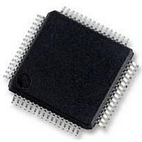
P89LPC9401FBD NXP Semiconductors, P89LPC9401FBD Datasheet - Page 9

P89LPC9401FBD
Manufacturer Part Number
P89LPC9401FBD
Description
IC, MCU 8BIT 80C51, LCD DRIVER, SMD
Manufacturer
NXP Semiconductors
Datasheet
1.P89LPC9401FBD551.pdf
(59 pages)
Specifications of P89LPC9401FBD
Controller Family/series
(8051) 8052
Core Size
8bit
No. Of I/o's
23
Program Memory Size
8KB
Ram Memory Size
256Byte
Cpu Speed
18MHz
Oscillator Type
External, Internal
No. Of Timers
4
No.
RoHS Compliant
Available stocks
Company
Part Number
Manufacturer
Quantity
Price
Part Number:
P89LPC9401FBD
Manufacturer:
NXP/恩智浦
Quantity:
20 000
Company:
Part Number:
P89LPC9401FBD,551
Manufacturer:
NXP Semiconductors
Quantity:
10 000
Company:
Part Number:
P89LPC9401FBD,557
Manufacturer:
NXP Semiconductors
Quantity:
10 000
Company:
Part Number:
P89LPC9401FBDЈ¬551
Manufacturer:
NXP
Quantity:
3 048
Philips Semiconductors
Table 3:
P89LPC9401_1
Preliminary data sheet
Symbol
P1.5/RST
P1.6
P1.7
P2.0 to P2.3,
P2.5
P2.0
P2.1
P2.2/MOSI
P2.3/MISO
P2.5/SPICLK
P3.0 to P3.1
P3.0/XTAL2/
CLKOUT
Pin description
Pin
11
10
9
6
7
18
19
20
14
…continued
Type Description
I
I
I/O
I/O
I/O
I/O
I/O
I/O
I/O
I/O
I/O
I/O
I/O
I/O
I/O
O
O
P1.5 — Port 1 bit 5 (input only).
RST — External Reset input during power-on or if selected via UCFG1. When
functioning as a reset input, a LOW on this pin resets the microcontroller, causing I/O
ports and peripherals to take on their default states, and the processor begins
execution at address 0. Also used during a power-on sequence to force ISP mode.
When using an oscillator frequency above 12 MHz, the reset input function of
P1.5 must be enabled. An external circuit is required to hold the device in reset at
power-up until V
removed V
using an oscillator frequency above 12 MHz, in some applications, an external
brownout detect circuit may be required to hold the device in reset when V
below the minimum specified operating range.
P1.6 — Port 1 bit 6.
P1.7 — Port 1 bit 7.
Port 2: Port 2 is an 5-bit I/O port with a user-configurable output type. During reset
Port 2 latches are configured in the input only mode with the internal pull-up disabled.
The operation of Port 2 pins as inputs and outputs depends upon the port configuration
selected. Each port pin is configured independently. Refer to
configurations”
All pins have Schmitt trigger inputs.
Port 2 also provides various special functions as described below:
P2.0 — Port 2 bit 0.
P2.1 — Port 2 bit 1.
P2.2 — Port 2 bit 2.
MOSI — SPI master out slave in. When configured as master, this pin is output; when
configured as slave, this pin is input.
P2.3 — Port 2 bit 3.
MISO — When configured as master, this pin is input, when configured as slave, this
pin is output.
P2.5 — Port 2 bit 5.
SPICLK — SPI clock. When configured as master, this pin is output; when configured
as slave, this pin is input.
Port 3: Port 3 is a 2-bit I/O port with a user-configurable output type. During reset
Port 3 latches are configured in the input only mode with the internal pull-up disabled.
The operation of Port 3 pins as inputs and outputs depends upon the port configuration
selected. Each port pin is configured independently. Refer to
configurations”
All pins have Schmitt triggered inputs.
Port 3 also provides various special functions as described below:
P3.0 — Port 3 bit 0.
XTAL2 — Output from the oscillator amplifier (when a crystal oscillator option is
selected via the flash configuration.
CLKOUT — CPU clock divided by 2 when enabled via SFR bit (ENCLK - TRIM.6). It
can be used if the CPU clock is the internal RC oscillator, watchdog oscillator or
external clock input, except when XTAL1/XTAL2 are used to generate clock source for
the RTC/system timer.
8-bit two-clock 80C51 microcontroller with 32 segment
DD
Rev. 01 — 5 September 2005
will fall below the minimum specified operating voltage. When
and
and
DD
Table 11 “Static electrical characteristics”
Table 11 “Static electrical characteristics”
has reached its specified level. When system power is
© Koninklijke Philips Electronics N.V. 2005. All rights reserved.
P89LPC9401
Section 7.13.1 “Port
Section 7.13.1 “Port
for details.
for details.
4 LCD driver
DD
9 of 59
falls


