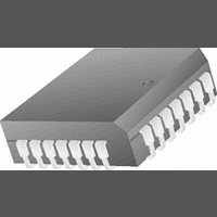
CS5102A-BL Cirrus Logic Inc, CS5102A-BL Datasheet - Page 30

CS5102A-BL
Manufacturer Part Number
CS5102A-BL
Description
A/D Converter (A-D) IC
Manufacturer
Cirrus Logic Inc
Specifications of CS5102A-BL
Input Channels Per Adc
2
Mounting Type
Surface Mount
No. Of Channels
2
Power Rating
44mW
Supply Voltage Min
4.5V
Peak Reflow Compatible (260 C)
No
Sample Rate
20kSPS
Supply Voltage Max
5.5V
Lead Free Status / RoHS Status
Contains lead / RoHS non-compliant
Available stocks
Company
Part Number
Manufacturer
Quantity
Price
Part Number:
CS5102A-BL
Manufacturer:
CRYSTAL
Quantity:
20 000
Company:
Part Number:
CS5102A-BLZ
Manufacturer:
Cirrus Logic Inc
Quantity:
10 000
Part Number:
CS5102A-BLZ
Manufacturer:
CRYSTAL
Quantity:
20 000
not limited by differential nonlinearities (DNL)
caused by calibration errors. Rather, the dominant
noise source is broadband thermal noise which
aliases into the baseband. This white broadband
noise also appears as an idle channel noise of
1/2 LSB (rms).
7.3
Like most discrete sample/hold amplifier designs,
the inherent sample/hold of the CS5101A and
CS5102A exhibits a frequency-dependent distor-
tion due to non-ideal sampling of the analog input
voltage. The calibrated capacitor array used during
conversions is also used to track and hold the an-
alog input signal. The conversion is not performed
on the analog input voltage per se, but is actually
performed on the charge trapped on the capacitor
array at the moment the HOLD command is given.
The charge on the array ideally assumes a linear
relationship to the analog input voltage. Any devia-
tion from this linear relationship will result in con-
30
Sampling Distortion
version errors even if the conversion process
proceeds flawlessly.
At DC, the DAC capacitor array's voltage coeffi-
cient dictates the converter's linearity. This varia-
tion in capacitance with respect to applied signal
voltage yields a nonlinear relationship between the
charge on the array and the analog input voltage
and places a bow or wave in the transfer function.
This is the dominant source of distortion at low in-
put frequencies (Figures 19, 20, 21, and 22).
The ideal relationship between the charge on the
array and the input voltage can also be distorted at
high signal frequencies due to nonlinearities in the
internal MOS switches. Dynamic signals cause ac
current to flow through the switches connecting the
capacitor array to the analog input pin in the track
mode. Nonlinear on-resistance in the switches
causes a nonlinear voltage drop. This effect wors-
ens with increased signal frequency and slew rate.
This distortion is negligible at signal levels below -
10 dB of full scale.
CS5101A CS5102A
DS45F6


