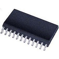
CS5460A-BS Cirrus Logic Inc, CS5460A-BS Datasheet - Page 28

CS5460A-BS
Manufacturer Part Number
CS5460A-BS
Description
Driver IC
Manufacturer
Cirrus Logic Inc
Datasheet
1.CS5460A-BSZ.pdf
(54 pages)
Specifications of CS5460A-BS
Peak Reflow Compatible (260 C)
No
Supply Voltage Max
5V
Driver Case Style
SSOP
Leaded Process Compatible
No
Mounting Type
Surface Mount
Package / Case
24-SSOP
Mounting Style
SMD/SMT
Lead Free Status / RoHS Status
Contains lead / RoHS non-compliant
Available stocks
Company
Part Number
Manufacturer
Quantity
Price
Part Number:
CS5460A-BS
Manufacturer:
CIRRUS
Quantity:
20 000
Company:
Part Number:
CS5460A-BSZ
Manufacturer:
CIRRUS
Quantity:
2
Company:
Part Number:
CS5460A-BSZR
Manufacturer:
CIRRUS
Quantity:
8 000
Part Number:
CS5460A-BSZR
Manufacturer:
CIRRUS
Quantity:
20 000
is explained in more detail in the following para-
graphs).
3.8.2 The Calibration Registers
Refer to Figure 3 and Figure 21.
Voltage Channel DC Offset Register and Cur-
rent Channel DC Offset Register - Store additive
correction values that are used to correct for DC
offsets which may be present on the voltage/cur-
rent channels within the entire meter system.
These registers are updated by the CS5460A after
a DC offset calibration sequence has been execut-
ed.
Voltage Channel Gain Register and Current
Channel Gain Register - Store the multiplicative
correction values determined by the full-scale gain
calibration signals that are applied to the meter’s
voltage/current channels. These registers are up-
dated by the CS5460A after either an AC or DC
gain calibration sequence has been executed.
Voltage Channel AC Offset Register and Cur-
rent Channel AC Offset Register - Store additive
offset correction values that are used to correct for
AC offsets which may be created on the volt-
age/current channels within the entire meter sys-
tem. Although a noise signal may have an average
value of zero [no DC offset] the noise may still have
a non-zero rms value, which can add an undesir-
able offset in the CS5460A’s Irms and Vrms re-
sults.
CS5460A after an AC offset calibration sequence
has been executed.
Referring to Figure 3, one should note that the AC
offset registers affect the output results differently
than the DC offset registers. The DC offset values
are applied to the voltage/current signals very early
in the signal path; the DC offset register value af-
fects all CS5460A results. This is not true for the
AC offset correction. The AC offset registers only
affect the results of the rms-voltage/rms-current
calculations.
Referring to Figure 3, the reader should note that
there are separate calibration registers for the AC
and DC offset corrections (for each channel). This
is not true for gain corrections, as there is only one
gain register per channel--AC and DC gain calibra-
tion results are stored in the same register. The re-
28
These registers are updated by the
sults in the gain registers reflect either the AC or
DC gain calibration results, whichever was per-
formed most recently. Therefore, both a DC and
AC offset can be applied to a channel at the same
time, but only one gain calibration can be applied
to each channel. Either AC or DC gain calibration
can be used, but not both.
For both the voltage channel and the current chan-
nel, while the AC offset calibration sequence per-
forms an entirely different function than the DC
offset calibration sequence, the AC gain and DC
gain calibration sequences perform the same func-
tion (but they accomplish the function using differ-
ent techniques).
Since both the voltage and current channels have
separate offset and gain registers associated with
them, system offset or system gain can be per-
formed on either channel without the calibration
results from one channel affecting the other.
3.8.3 Calibration Sequence
1. The CS5460A must be operating in its active
state, and ready to accept valid commands via the
SPI interface, before a calibration sequence can
be executed. Clearing the ‘DRDY’ bit in the Status
Register is also recommended.
2. Apply appropriate calibration signal(s) to the “+”
and “-” signals of the voltage/current channel input
pairs. (The appropriate calibration signals for each
type of calibration sequence are discussed next, in
Sections 3.8.4 and 3.8.5.). The recommended se-
quence of calibration, if both gain and offset cali-
bration are required, is to run offset calibration
before gain calibration; and if both AC and DC off-
set calibration are required, DC offset should be
calibrated first.
3. Next send the 8-bit calibration command to the
CS5460A serial interface.
4. After the CS5460A has finished running the de-
sired internal calibration sequence and has stored
the updated calibration results in the appropriate
calibration registers, the DRDY bit is set in the Sta-
tus Register to indicate that the calibration se-
quence has been completed. If desired, the results
of the calibration can now be read from the appro-
priate gain/offset registers, via the serial port.
CS5460A
DS487F4


