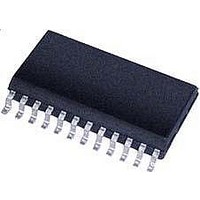
CS5460A-BS Cirrus Logic Inc, CS5460A-BS Datasheet - Page 35

CS5460A-BS
Manufacturer Part Number
CS5460A-BS
Description
Driver IC
Manufacturer
Cirrus Logic Inc
Datasheet
1.CS5460A-BSZ.pdf
(54 pages)
Specifications of CS5460A-BS
Peak Reflow Compatible (260 C)
No
Supply Voltage Max
5V
Driver Case Style
SSOP
Leaded Process Compatible
No
Mounting Type
Surface Mount
Package / Case
24-SSOP
Mounting Style
SMD/SMT
Lead Free Status / RoHS Status
Contains lead / RoHS non-compliant
Available stocks
Company
Part Number
Manufacturer
Quantity
Price
Part Number:
CS5460A-BS
Manufacturer:
CIRRUS
Quantity:
20 000
Company:
Part Number:
CS5460A-BSZ
Manufacturer:
CIRRUS
Quantity:
2
Company:
Part Number:
CS5460A-BSZR
Manufacturer:
CIRRUS
Quantity:
8 000
Part Number:
CS5460A-BSZR
Manufacturer:
CIRRUS
Quantity:
20 000
Note also that in addition to the time-constants of
the input R-C filters, the phase-shifting properties
of the voltage/current sensors devices may also
contribute to the overall time-constants of the volt-
age/current input sensor networks. For example,
current-sense transformers and potential trans-
formers can impose phase-shifts on the sensed
current/voltage waveforms. Therefore, this possi-
ble source of additional phase-shift caused by sen-
sor devices may also need to be considered while
selecting the final R and C values for the volt-
age/current anti-aliasing filters. As an alternative
to, or in addition to the fine adjustment of the R and
C values of the two anti-alias filters, the CS5460A’s
phase compensation bits (see Phase Compensa-
tion) can also be adjusted, in order to more closely
match the overall time-constants of the volt-
age/current input networks. Regardless of whether
the phase compensation bits are or are not used to
help more closely match the time-constants, this
requirement of equal time-constants must ulti-
mately be considered when selecting the final R
and C values that will be used for the input filters.
(Of course, this factor may not turn out to be so im-
portant if the designer is confident that the
mis-match between the voltage/current channel
time-constants will not cause enough error to vio-
late the accuracy requirements for the given pow-
er/energy metering application.)
3. Referring to the specs in Section 1, note that the
differential input impedance across the current
channel input pins is only 30 kΩ, which is signifi-
cantly less than the corresponding impedance
across the voltage channel input pins (which is
1 MΩ). While the impedance across the voltage
channel is usually high enough to be ignored, the
impedance across the current channel inputs may
need to be taken into account by the designer
when the desired cutoff frequencies of the filters
(and the time-constants of the overall input net-
works) are computed. Also, because of this rather
low input impedance across the current channel in-
puts, the designer should note that as the values
for R
the current channel’s input impedance can begin to
cause a significant voltage drop within the current
channel input network. If this is not taken into ac-
count, values may be chosen for R
large enough to cause a discrepancy between the
DS487F4
I+
and/or R
I-
are increased, the interaction of
I+
= R
I-
that are
expected (theoretical) sensor gain and the actual
sensor gain of the current sensor network, which
may not be anticipated by the designer. Also, if this
voltage drop effect is not considered, the designer
may select values for R
larger than they should be, in terms of maximizing
the available dynamic range of the current channel
input. For the very same reason, the line-cur-
rent-to-sensor-output-voltage conversion factor of
the current sensor may not be optimized if this volt-
age division is not considered, when (for example)
selecting a value for the burden resistor for a given
current transformer. This issue should be consid-
ered, although a slight voltage drop only causes a
slight loss in available dynamic range, and the ef-
fects of this voltage drop on the actual current
channel sensor gain can be removed during gain
calibration of the current channel.
4. Referring to Figures 6 - 9, not all of the capaci-
tors/resistors shown in these example circuit dia-
grams are necessary; however, note that the all of
the filter capacitors (C
diff
ability of both input networks to attenuate very
high-frequency RFI that can enter into the
CS5460A’s analog input pins. Therefore, during
layout of the PCB, these capacitors should be
placed in close proximity to their respective input
pins.
If any/all of the common-mode connected capaci-
tors (C
works, their values should be selected such that
they are at least one order of magnitude smaller
than the value of the differential capacitors (C
and C
a) The value tolerance for most types of commer-
cially available surface-mount capacitors is not
small enough to insure appreciable value match-
ing, between the value of C
between the value of C
match can adversely affect the desired differen-
tial-mode response of the voltage/current input
networks. By keeping the values of these com-
mon-mode capacitors small, and allowing the val-
ue of the C
differential 1st-order time-constant of the input filter
networks, this undesirable possibility of frequency
response variation can be minimized.
) can, in some situations, help to improve the
Idiff
V+
, C
). This is done for at least two reasons:
V-
, C
Vdiff
I+
, C
, and C
I-
) are included in the input net-
V+
V+
, C
I+
vs. C
V-
and R
Idiff
, C
V+
I+
V-
vs. C
to dominate the
, C
. Such value mis-
I
that are slightly
I-
CS5460A
, C
V-
, as well as
Vdiff
, and C
Vdiff
35
I-
,


