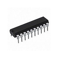
DAC0832LCN National Semiconductor, DAC0832LCN Datasheet - Page 10

DAC0832LCN
Manufacturer Part Number
DAC0832LCN
Description
D/A Converter (D-A) IC
Manufacturer
National Semiconductor
Datasheet
1.DAC0832LCN.pdf
(28 pages)
Specifications of DAC0832LCN
Resolution (bits)
8bit
Data Interface
CMOS, Parallel, TTL
No. Of Pins
20
Settling Time
1µs
Mounting Type
Through Hole
Peak Reflow Compatible (260 C)
No
No. Of Bits
8 Bit
Leaded Process Compatible
No
Number Of Channels
1
Resolution
8b
Interface Type
Parallel
Single Supply Voltage (typ)
Not RequiredV
Dual Supply Voltage (typ)
Not RequiredV
Architecture
R-2R
Power Supply Requirement
Digital
Output Type
Current
Integral Nonlinearity Error
0.2LSB
Single Supply Voltage (min)
Not RequiredV
Single Supply Voltage (max)
Not RequiredV
Dual Supply Voltage (min)
Not RequiredV
Dual Supply Voltage (max)
Not RequiredV
Operating Temp Range
0C to 70C
Operating Temperature Classification
Commercial
Mounting
Through Hole
Pin Count
20
Package Type
PDIP
Lead Free Status / RoHS Status
Contains lead / RoHS non-compliant
Lead Free Status / RoHS Status
Contains lead / RoHS non-compliant
Available stocks
Company
Part Number
Manufacturer
Quantity
Price
Company:
Part Number:
DAC0832LCN
Manufacturer:
NS
Quantity:
6 000
Company:
Part Number:
DAC0832LCN
Manufacturer:
NS
Quantity:
6 000
Part Number:
DAC0832LCN
Manufacturer:
NS/国半
Quantity:
20 000
www.national.com
DAC0830 Series Application Hints
*
The ILE pin is an active high chip select which can be
decoded from the address bus as a qualifier for the normal
CS signal generated during a write operation. This can be
used to provide a higher degree of decoding unique control
signals for a particular DAC, and thereby create a more
efficient addressing scheme.
Another useful application of the ILE pin of each DAC in a
multiple DAC system is to tie these inputs together and use
this as a control line that can effectively “freeze” the outputs
of all the DAC’s at their present value. Pulling this line low
latches the input register and prevents new data from being
TIE TO LOGIC 1 IF NOT NEEDED (SEE SEC. 1.1).
FIGURE 2. Controlling Mutiple DACs
FIGURE 3.
(Continued)
10
written to the DAC. This can be particularly useful in multi-
processing systems to allow a processor other than the one
controlling the DAC’s to take over control of the data bus and
control lines. If this second system were to use the same
addresses as those decoded for DAC control (but for a
different purpose) the ILE function would prevent the DAC’s
from being erroneously altered.
In a “Stand-Alone” system the control signals are generated
by discrete logic. In this case double-buffering can be con-
trolled by simply taking CS and XFER to a logic “0”, ILE to a
logic “1” and pulling WR
1
low to load data to the input latch.
00560835
00560836


