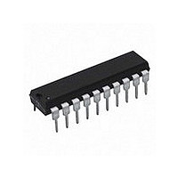
DAC0832LCN National Semiconductor, DAC0832LCN Datasheet - Page 13

DAC0832LCN
Manufacturer Part Number
DAC0832LCN
Description
D/A Converter (D-A) IC
Manufacturer
National Semiconductor
Datasheet
1.DAC0832LCN.pdf
(28 pages)
Specifications of DAC0832LCN
Resolution (bits)
8bit
Data Interface
CMOS, Parallel, TTL
No. Of Pins
20
Settling Time
1µs
Mounting Type
Through Hole
Peak Reflow Compatible (260 C)
No
No. Of Bits
8 Bit
Leaded Process Compatible
No
Number Of Channels
1
Resolution
8b
Interface Type
Parallel
Single Supply Voltage (typ)
Not RequiredV
Dual Supply Voltage (typ)
Not RequiredV
Architecture
R-2R
Power Supply Requirement
Digital
Output Type
Current
Integral Nonlinearity Error
0.2LSB
Single Supply Voltage (min)
Not RequiredV
Single Supply Voltage (max)
Not RequiredV
Dual Supply Voltage (min)
Not RequiredV
Dual Supply Voltage (max)
Not RequiredV
Operating Temp Range
0C to 70C
Operating Temperature Classification
Commercial
Mounting
Through Hole
Pin Count
20
Package Type
PDIP
Lead Free Status / RoHS Status
Contains lead / RoHS non-compliant
Lead Free Status / RoHS Status
Contains lead / RoHS non-compliant
Available stocks
Company
Part Number
Manufacturer
Quantity
Price
Company:
Part Number:
DAC0832LCN
Manufacturer:
NS
Quantity:
6 000
Company:
Part Number:
DAC0832LCN
Manufacturer:
NS
Quantity:
6 000
Part Number:
DAC0832LCN
Manufacturer:
NS/国半
Quantity:
20 000
DAC0830 Series Application Hints
Always use the internal R
voltage since this resistor matches (and tracks with tempera-
ture) the value of the resistors used to generate the output
current (I
2.3 Op Amp Considerations
The op amp used in Figure 7 should have offset voltage
nulling capability (See Section 2.5).
The selected op amp should have as low a value of input
bias current as possible. The product of the bias current
times the feedback resistance creates an output voltage
error which can be significant in low reference voltage appli-
cations. BI-FET
with these DACs because of their very low input current.
Transient response and settling time of the op amp are
important in fast data throughput applications. The largest
stability problem is the feedback pole created by the feed-
back resistance, R
This appears from the op amp output to the (−) input and
includes the stray capacitance at this node. Addition of a
lead capacitance, C
and ringing at the output for a step change in DAC output
current.
Finally, the output voltage swing of the amplifier must be
greater than V
voltage. Depending on the loading on the output of the
amplifier and the available op amp supply voltages (only
volts in many development systems), a reference voltage
less than 10 volts may be necessary to obtain the full analog
output voltage range.
(Continued)
OUT1
).
REF
™
op amps are highly recommended for use
fb
, and the output capacitance of the DAC.
C
to allow reaching the full scale output
in Figure 8 , greatly reduces overshoot
fb
resistor to create an output
00560837
00560838
±
12
FIGURE 6.
FIGURE 7.
13
2.4 Bipolar Output Voltage with a Fixed Reference
The addition of a second op amp to the previous circuitry can
be used to generate a bipolar output voltage from a fixed
reference voltage. This, in effect, gives sign significance to
the MSB of the digital input word and allows two-quadrant
multiplication of the reference voltage. The polarity of the
reference can also be reversed to realize full 4-quadrant
multiplication:
shown in Figure 9 .
This configuration features several improvements over exist-
ing circuits for bipolar outputs with other multiplying DACs.
Only the offset voltage of amplifier 1 has to be nulled to
preserve linearity of the DAC. The offset voltage error of the
second op amp (although a constant output voltage error)
has no effect on linearity. It should be nulled only if absolute
output accuracy is required. Finally, the values of the resis-
tors around the second amplifier do not have to match the
internal DAC resistors, they need only to match and tem-
perature track each other. A thin film 4-resistor network
available from Beckman Instruments, Inc. (part no.
694-3-R10K-D) is ideally suited for this application. These
resistors are matched to 0.1% and exhibit only 5 ppm/˚C
resistance tracking temperature coefficient. Two of the four
available 10 k
Figure 9 and the other two can be used independently as the
resistances labeled 2R.
±
V
REF
resistors can be paralleled to form R in
x
±
Digital Code=
±
V
OUT
. This circuit is
www.national.com


