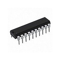
DAC0832LCN National Semiconductor, DAC0832LCN Datasheet - Page 12

DAC0832LCN
Manufacturer Part Number
DAC0832LCN
Description
D/A Converter (D-A) IC
Manufacturer
National Semiconductor
Datasheet
1.DAC0832LCN.pdf
(28 pages)
Specifications of DAC0832LCN
Resolution (bits)
8bit
Data Interface
CMOS, Parallel, TTL
No. Of Pins
20
Settling Time
1µs
Mounting Type
Through Hole
Peak Reflow Compatible (260 C)
No
No. Of Bits
8 Bit
Leaded Process Compatible
No
Number Of Channels
1
Resolution
8b
Interface Type
Parallel
Single Supply Voltage (typ)
Not RequiredV
Dual Supply Voltage (typ)
Not RequiredV
Architecture
R-2R
Power Supply Requirement
Digital
Output Type
Current
Integral Nonlinearity Error
0.2LSB
Single Supply Voltage (min)
Not RequiredV
Single Supply Voltage (max)
Not RequiredV
Dual Supply Voltage (min)
Not RequiredV
Dual Supply Voltage (max)
Not RequiredV
Operating Temp Range
0C to 70C
Operating Temperature Classification
Commercial
Mounting
Through Hole
Pin Count
20
Package Type
PDIP
Lead Free Status / RoHS Status
Contains lead / RoHS non-compliant
Lead Free Status / RoHS Status
Contains lead / RoHS non-compliant
Available stocks
Company
Part Number
Manufacturer
Quantity
Price
Company:
Part Number:
DAC0832LCN
Manufacturer:
NS
Quantity:
6 000
Company:
Part Number:
DAC0832LCN
Manufacturer:
NS
Quantity:
6 000
Part Number:
DAC0832LCN
Manufacturer:
NS/国半
Quantity:
20 000
www.national.com
DAC0830 Series Application Hints
2.0 ANALOG CONSIDERATIONS
The fundamental purpose of any D to A converter is to
provide an accurate analog output quantity which is repre-
sentative of the applied digital word. In the case of the
DAC0830, the output, I
to the product of the applied reference voltage and the digital
input word. For application versatility, a second output,
I
complement of the digital input. Basically:
where the digital input is the decimal (base 10) equivalent of
the applied 8-bit binary word (0 to 255), V
at pin 8 and 15 k
resistance, R, of the R-2R ladder network (discussed in
Section 2.1).
Several factors external to the DAC itself must be consid-
ered to maintain analog accuracy and are covered in subse-
quent sections.
2.1 The Current Switching R-2R Ladder
The analog circuitry, Figure 6 , consists of a silicon-chromium
(SiCr or Si-chrome) thin film R-2R ladder which is deposited
on the surface oxide of the monolithic chip. As a result, there
are no parasitic diode problems with the ladder (as there
may be with diffused resistors) so the reference voltage,
V
5V
OUT2
REF
DC
, can range −10V to +10V even if V
, is provided as a current directly proportional to the
.
is the nominal value of the internal
OUT1
, is a current directly proportional
FIGURE 5. Accommodating a High Speed System
CC
REF
for the device is
is the voltage
00560808
(Continued)
12
The digital input code to the DAC simply controls the position
of the SPDT current switches and steers the available ladder
current to either I
input level (“1” or “0”) respectively, as shown in Figure 6 . The
MOS switches operate in the current mode with a small
voltage drop across them and can therefore switch currents
of either polarity. This is the basis for the 4-quadrant multi-
plying feature of this DAC.
2.2 Basic Unipolar Output Voltage
To maintain linearity of output current with changes in the
applied digital code, it is important that the voltages at both
of the current output pins be as near ground potential (0V
as possible. With V
either I
most applications this output current is converted to a volt-
age by using an op amp as shown in Figure 7 .
The inverting input of the op amp is a “virtual ground” created
by the feedback from its output through the internal 15 k
resistor, R
digital input and the reference voltage) will flow through R
to the output of the amplifier. Two-quadrant operation can be
obtained by reversing the polarity of V
to flow into the DAC and be sourced from the output of the
amplifier. The output voltage, in either case, is always equal
to I
voltage.
The reference can be either a stable DC voltage source or
an AC signal anywhere in the range from −10V to +10V. The
DAC can be thought of as a digitally controlled attenuator:
the output voltage is always less than or equal to the applied
reference voltage. The V
a nominal impedance of 15 k to ground to external circuitry.
OUT1
OUT1
xR
fb
fb
. All of the output current (determined by the
or I
and is the opposite polarity of the reference
OUT2
OUT1
REF
will cause a 0.01% linearity error. In
or I
=+10V every millivolt appearing at
REF
OUT2
terminal of the device presents
as determined by the logic
REF
thus causing I
OUT1
DC
fb
)


