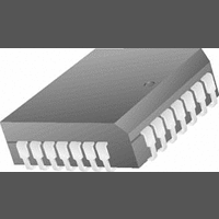
LM12H458CIV National Semiconductor, LM12H458CIV Datasheet - Page 34

LM12H458CIV
Manufacturer Part Number
LM12H458CIV
Description
A/D Converter (A-D) IC
Manufacturer
National Semiconductor
Datasheet
1.LM12H458CIV.pdf
(36 pages)
Specifications of LM12H458CIV
No. Of Pins
28
Peak Reflow Compatible (260 C)
No
Supply Voltage
5V
Supply Voltage Max
5V
No. Of Bits
12 Bit
Leaded Process Compatible
No
Mounting Type
Surface Mount
No. Of Channels
1
Number Of Elements
1
Sample Rate
182KSPS
Input Polarity
Bipolar
Input Type
Voltage
Rated Input Volt
±5V
Differential Input
Yes
Power Supply Requirement
Analog and Digital
Single Supply Voltage (typ)
5V
Single Supply Voltage (min)
3V
Single Supply Voltage (max)
5.5V
Dual Supply Voltage (typ)
Not RequiredV
Dual Supply Voltage (min)
Not RequiredV
Dual Supply Voltage (max)
Not RequiredV
Differential Linearity Error
±0.75LSB
Integral Nonlinearity Error
±1LSB
Operating Temp Range
-40C to 85C
Operating Temperature Classification
Industrial
Mounting
Surface Mount
Pin Count
44
Package Type
PLCC
Lead Free Status / RoHS Status
Contains lead / RoHS non-compliant
Lead Free Status / RoHS Status
Contains lead / RoHS non-compliant
Available stocks
Company
Part Number
Manufacturer
Quantity
Price
Company:
Part Number:
LM12H458CIV
Manufacturer:
Texas Instruments
Quantity:
10 000
Part Number:
LM12H458CIV
Manufacturer:
NS/国半
Quantity:
20 000
Company:
Part Number:
LM12H458CIV/NOPB
Manufacturer:
National Semiconductor
Quantity:
135
Company:
Part Number:
LM12H458CIV/NOPB
Manufacturer:
Intersil
Quantity:
188
Company:
Part Number:
LM12H458CIV/NOPB
Manufacturer:
Texas Instruments
Quantity:
10 000
Company:
Part Number:
LM12H458CIVF
Manufacturer:
Texas Instruments
Quantity:
10 000
www.national.com
6.0 Design Considerations
niques). Failure to do so can result in erratic operation.
Generally, a series 30Ω to 50Ω resistor in the clock line,
located as close to the clock source as possible, will prevent
most problems. The clock source should drive ONLY the
LM12(H)458 clock pin.
7.0 Common Application Problems
Driving the analog inputs with op-amp(s) powered from
supplies other than the supply used for the LM12(H)458.
This practice allows for the possibility of the amplifier output
(LM12(H)458 input) to reach potentials outside of the 0V to
V
amplifier use supply voltages outside of the range of the
LM12(H)458 supply rails. This could also happen upon
power up if the amplifier supply or supplies ramp up faster
than the supply of the LM12(H)458. If any pin experiences a
potential more than 100 mV below ground or above the
supply voltage, even on a fast transient basis, the result
could be erratic operation, missing codes, one channel in-
teracting with one or more of the others, skipping channels
or a complete malfunction, depending upon how far the input
is driven beyond the supply rails.
Not performing a full calibration at power up. This can
result in missing codes. The device needs to have a full
calibration run and completed after power up and BEFORE
attempting to perform even a single conversion or watchdog
operation. The only way to recover if this is violated is to
interrupt the power to the device.
Not waiting for the calibration process to complete be-
fore trying to write to the device. Once a calibration is
requested, the ONLY read of the LM12(H)458 should be if
the Interrupt Status Register to check for a completed cali-
bration. Attempting a write or any other read during calibra-
tion would cause a corruption of the calibration process,
resulting in missing codes. The only way to recover would be
to interrupt the power.
A
+ range. This could happen in normal operation if the
(Continued)
34
Improper termination of digital lines. Improper termination
can result in energy reflections that build up to cause over-
shoot that goes above the supply potential and undershoot
that goes below ground. It is never good to drive a device
beyond the supply rails, unless the device is specifically
designed to handle this situation, but the LM12(H)458 is
more sensitive to this condition that most devices. Again, if
any pin experiences a potential more than 100 mV below
ground or above the supply voltage, even on a fast transient
basis, the result could be erratic operation, missing codes, or
a complete malfunction, depending upon how far the input is
driven beyond the supply rails. The clock input is the most
sensitive digital one. Generally, a 50Ω series resistor, lo-
cated very close to the signal source, will keep digital lines
"clean".
Excessive output capacitance on the digital lines. The
current required to charge the capacitance on the digital
outputs can cause noise on the supply bus within the
LM12(H)458, causing internal supply "bounce" even when
the external supply pin is pretty stable. The current required
to discharge the output capacitance can cause die ground
"bounce". Either of these can cause noise to be induced at
the analog inputs, resulting in conversion errors.
Output capacitance should be limited as much as possible. A
series 100Ω resistor in each digital output line, located very
close to the output pin, will limit the charge and discharge
current, minimizing the extent of the conversion errors.
Improper CS decoding. If address decoder is used, care
must be exercised to ensure that no "runt" (very narrow)
pulse is produced on theCS line when trying to address
another device or memory. Even sub-nanosecond spikes on
the CS line can cause the chip to be reprogrammed in
accordance with what happens to be on the data lines at the
time. The result is unexpected operation. The worst case
result is that the device is put into the "Test" mode and the
on-board EEPROM that corrects linearity is corrupted. If this
happens, the only recourse is to replace the device.


