LMC662CN National Semiconductor, LMC662CN Datasheet - Page 2
LMC662CN
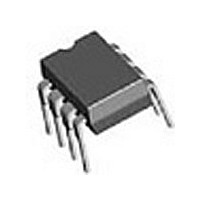
Manufacturer Part Number
LMC662CN
Description
Operational Amplifier (Op-Amp) IC
Manufacturer
National Semiconductor
Type
General Purpose Amplifierr
Datasheet
1.LMC662CN.pdf
(14 pages)
Specifications of LMC662CN
No. Of Amplifiers
2
Slew Rate
1.1V/µs
No. Of Pins
8
Peak Reflow Compatible (260 C)
No
Leaded Process Compatible
No
Mounting Type
Through Hole
Package / Case
8-DIP
Rail/rail I/o Type
Rail to Rail Output
Number Of Elements
2
Unity Gain Bandwidth Product
1.4MHz
Common Mode Rejection Ratio
63dB
Input Offset Voltage
6mV
Input Bias Current
2fA
Single Supply Voltage (typ)
5/9/12/15V
Dual Supply Voltage (typ)
Not RequiredV
Voltage Gain In Db
126.02dB
Power Supply Rejection Ratio
63dB
Power Supply Requirement
Single
Shut Down Feature
No
Single Supply Voltage (min)
4.75V
Single Supply Voltage (max)
15.5V
Dual Supply Voltage (min)
Not RequiredV
Dual Supply Voltage (max)
Not RequiredV
Technology
CMOS
Operating Temp Range
0C to 70C
Operating Temperature Classification
Commercial
Mounting
Through Hole
Pin Count
8
Package Type
PDIP
Lead Free Status / RoHS Status
Contains lead / RoHS non-compliant
Lead Free Status / RoHS Status
Contains lead / RoHS non-compliant
Available stocks
Company
Part Number
Manufacturer
Quantity
Price
Company:

Part Number:
LMC662CN
Manufacturer:
NSC
Quantity:
1 200
Part Number:
LMC662CN
Manufacturer:
NS/国半
Quantity:
20 000
Company:
Part Number:
LMC662CN/AIN
Manufacturer:
NSC
Quantity:
5 510
Company:
Part Number:
LMC662CN/IN/AIN
Manufacturer:
NSC
Quantity:
5 510
Company:
Part Number:
LMC662CN/ISMDIN
Manufacturer:
KIA
Quantity:
5 510


www.national.com
Absolute Maximum Ratings
If Military/Aerospace specified devices are required,
please contact the National Semiconductor Sales Office/
Distributors for availability and specifications.
DC Electrical Characteristics
Differential Input Voltage
Supply Voltage (V
Output Short Circuit to V
Output Short Circuit to V
Lead Temperature
Storage Temp. Range
Voltage at Input/Output Pins
Current at Output Pin
Current at Input Pin
Current at Power Supply Pin
Input Offset Voltage
Input Offset Voltage
Average Drift
Input Bias Current
Input Offset Current
Input Resistance
Common Mode
Rejection Ratio
Positive Power Supply
Rejection Ratio
Negative Power Supply
Rejection Ratio
Input Common-Mode
Voltage Range
Large Signal
Voltage Gain
Unless otherwise specified, all limits guaranteed for T
V
(Soldering, 10 sec.)
−
= 0V, V
Parameter
CM
= 1.5V, V
+
− V
−
)
+
−
O
= 2.5V and R
0V ≤ V
V
5V ≤ V
V
0V ≤ V
V
For CMRR ≥ 50 dB
R
Sourcing
Sinking
R
Sourcing
Sinking
+
O
+
L
L
(V
= 15V
= 5V & 15V
= 2 kΩ (Note 5)
= 600Ω (Note 5)
= 2.5V
+
Conditions
) +0.3V, (V
CM
+
−
−65˚C to +150˚C
±
≤ 15V
≤ −10V
L
Supply Voltage
≤ 12.0V
>
1M unless otherwise specified.
(Note 3)
(Note 12)
−
(Note 1)
±
) −0.3V
±
18 mA
35 mA
260˚C
5 mA
16V
J
= 25˚C. Boldface limits apply at the temperature extremes. V
2
V
(Note 4)
0.002
0.001
+
2000
1000
−0.4
Typ
500
250
1.3
>
Operating Ratings
83
83
94
− 1.9
1
Power Dissipation
Junction Temperature
ESD Tolerance (Note 8)
Temperature Range
Supply Voltage Range
Power Dissipation
Thermal Resistance (θ
1
LMC662AI
LMC662C
8-Pin Molded DIP
8-Pin SO
LMC662AI
V
V
(Note 4)
Limit
+
+
−0.1
440
400
180
120
220
200
100
3.3
70
68
70
68
84
83
60
− 2.3
− 2.5
3
4
2
0
JA
) (Note 11)
(Note 3)
LMC662C
V
V
(Note 4)
+
+
Limit
−0.1
300
200
150
100
6.3
63
62
63
62
74
73
90
80
50
40
− 2.3
− 2.4
6
2
1
0
−40˚C ≤ T
0˚C ≤ T
4.75V to 15.5V
J
J
(Note 10)
101˚C/W
165˚C/W
(Note 2)
≤ +85˚C
≤ +70˚C
TeraΩ
1000V
Units
µV/˚C
V/mV
V/mV
V/mV
V/mV
+
150˚C
max
max
max
max
min
min
min
min
min
min
min
min
mV
pA
pA
dB
dB
dB
= 5V,
V
V
Related parts for LMC662CN
Image
Part Number
Description
Manufacturer
Datasheet
Request
R

Part Number:
Description:
National Semiconductor [8-Bit D/A Converter]
Manufacturer:
National Semiconductor
Datasheet:
Part Number:
Description:
National Semiconductor [Media Coprocessor]
Manufacturer:
National Semiconductor
Datasheet:
Part Number:
Description:
Digitally Controlled Tone and Volume Circuit with Stereo Audio Power Amplifier, Microphone Preamp Stage and National 3D Sound
Manufacturer:
National Semiconductor
Datasheet:
Part Number:
Description:
Digitally Controlled Tone and Volume Circuit with Stereo Audio Power Amplifier, Microphone Preamp Stage and National 3D Sound
Manufacturer:
National Semiconductor
Datasheet:
Part Number:
Description:
AC97 Rev 2 Codec with Sample Rate Conversion and National 3D Sound
Manufacturer:
National Semiconductor
Part Number:
Description:
Manufacturer:
National Semiconductor
Datasheet:
Part Number:
Description:
Manufacturer:
National Semiconductor
Datasheet:
Part Number:
Description:
General Purpose, Low Voltage, Low Power, Rail-to-Rail Output Operational Amplifiers
Manufacturer:
National Semiconductor
Datasheet:
Part Number:
Description:
8-bit 20 MSPS flash A/D converter.
Manufacturer:
National Semiconductor
Datasheet:
Part Number:
Description:
Low Noise Quad Operational Amplifier
Manufacturer:
National Semiconductor
Datasheet:
Part Number:
Description:
Quad Differential Line Receivers
Manufacturer:
National Semiconductor
Datasheet:
Part Number:
Description:
Quad High Speed Trapezoidal? Bus Transceiver
Manufacturer:
National Semiconductor
Datasheet:
Part Number:
Description:
Dual Line Receiver
Manufacturer:
National Semiconductor
Datasheet:
Part Number:
Description:
TTL to 10k ECL Level Translator with Latch
Manufacturer:
National Semiconductor
Datasheet: